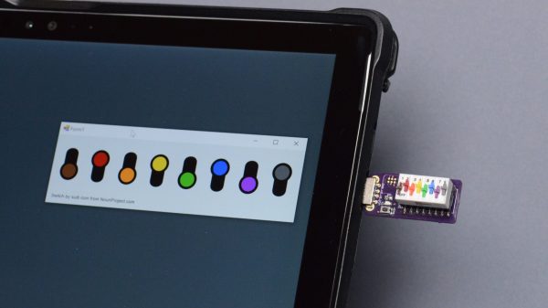
Oftentimes, when programming, we’ll put configuration switches into a config file in order to control the behaviour of our code. However, having to regularly open a text editor to make changes can be a pain. This colorful little DIP switch dongle from [Glen Aikins] makes for a fun alternative solution.
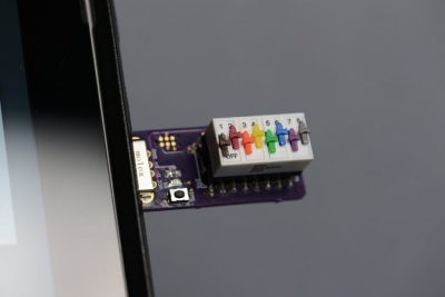
The build is simple, relying on a rainbow-colored 8-pin DIP switch as the core of the project. A PIC16F1459 then reads the position of the switches, with the 8-bit microcontroller doing the job of speaking USB to the host machine. The device enumerates as a USB HID device, and reports to the host machine when queried as to the state of its 8 switches. [Glen] used a basic C# app to show a digital representation of the switches on screen changing as per the real physical DIP switch plugged into the machine.
It’s a great tool for controlling up to 8 different parameters in a program you might be working on, without having to dive into your editor to change the relevant parts. Also, it bears noting that the rainbow design is simply very fetching and a cool thing to have plugged into your computer. It’s a more serious device than [Glen’s] hilarious 4-byte “solid state drive” that we saw recently, but we love them both all the same!