We’ve all spent the last year or more under the shadow of the COVID-19 pandemic, and though some of us may have been vaccinated or come through its various waves it remains far from over. One of the hardest-hit parts of the world at the moment is in India, where health services are struggling to maintain adequate oxygen supply such is the demand for it from sick patients.
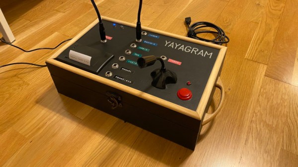
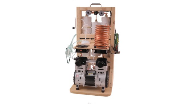
India’s hacker and maker community have risen to the challenge and done their bit to supply needed resources, and fresh from last year’s PPE manufacturing efforts a group from the Makers Asylum hackerspace in Goa have launched upon a fresh challenge. They aim to start producing the established open-source OxiKit oxygen concentrator in the Indian hackerspace community using locally manufactured parts, and they’ve launched a crowdfunding effort to cover their development, prototyping, and certification work.
The oxygen concentrator project builds on Makers Asylum’s experience last year as part of an extremely successful network of makerspaces producing PPE, which demonstrates that they have the resources, logistics, and ability to take on a project of this size. The OxiKit is no hare-brained contraption but an established and successful design that is already at work, so we believe that this project has a good chance of success. It’s close to home for Hackaday too, and one of the people involved with it is our colleague [Anool Mahidharia].
In a global pandemic only a global response can overcome the incredible challenges before us. For that reason we’d like to urge you to take a look at the Makers Asylum page wherever you are, and if you can, support it.
Continue reading “Indian Makers Respond To The COVID-19 Pandemic By Producing Oxygen Concentrators”