The trouble with fixing electronics is that most devices are just black boxes — literally. Tear it down, look inside, but it usually doesn’t matter — all you see are black epoxy blobs, taunting you with the fact that one or more of them are dead with no external indication of the culprit.
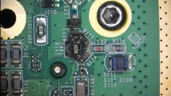
Sometimes, though, you get lucky, as [FeedbackLoop] did with this Rigol spectrum analyzer fix. The instrument powered up and sort of worked, but the noise floor was unacceptably high. Even before opening it up, there was clearly a problem; in general, spectrum analyzers shouldn’t rattle. Upon teardown, it was clear that someone had been inside before and got reassembly wrong, with a loose fastener and some obviously shorted components to show for it. But while the scorched remains of components made a great place to start diagnosis, it doesn’t mean the fix was going to be easy.
Figuring out the values of the nuked components required a little detective work. The blast zone seemed to once hold a couple of resistors, a capacitor, a set of PIN diodes, and a couple of tiny inductors. Also nearby were a pair of chips, sadly with the markings lasered off. With some online snooping and a little bit of common sense, [FeedbackLoop] was able to come up with plausible values for most of these — even the chips, which turned out to be HMC221 RF switches.
Cleaning up the board was a bit of a chore — the shorted components left quite a crater in the board, which was filled with CA glue, and a bunch of missing pads. This called for some SMD soldering heroics, which sadly didn’t fix the noise problem. Replacing the two RF switches and the PIN diodes seemed to fix the problem, albeit at the cost of some loss. Sometimes, good enough is good enough.
This isn’t the first time [FeedbackLoop] has gotten lucky with choice test equipment in need of repairs — this memory module transplant on a scopemeter comes to mind.
Continue reading “Putting The Magic Smoke Back Into A Dodgy Spectrum Analyzer”