By the turn of the 19th century, most scientists were convinced that the natural world was composed of atoms. [Einstein’s] 1905 paper on Brownian motion, which links the behavior of tiny particles suspended in a liquid to the movement of atoms put the nail in the coffin of the anti-atom crowd. No one could actually see atoms, however. The typical size of a single atom ranges from 30 to 300 picometers. With the wavelength of visible light coming in at a whopping 400 – 700 nanometers, it is simply not possible to “see” an atom. Not possible with visible light, that is. It was the summer of 1982 when Gerd Binnig and Heinrich Rohrer, two researchers at IBM’s Zurich Research Laboratory, show to the world the first ever visual image of an atomic structure. They would be awarded the Nobel prize in physics for their invention in 1986.
The Scanning Tunneling Microscope
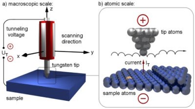
IBM’s Scanning Tunneling Microscope, or STM for short, uses an atomically sharp needle that passes over the surface of an (electrically conductive) object – the distance between the tip and object being just a few hundred picometers, or the diameter of a large atom.
Continue reading “Quantum Mechanics In Your Processor: Tunneling And Transistors”