Changing Color Under Pressure

When you saw the picture for this article, did you think of a peacock’s feather? These fibers are not harvested from birds, and in fact, the colors come from transparent rubber. As with peacock feathers, they come from the way light reflects off layers of differing materials, this is known as optical interference, and it is the same effect seen on oil slicks. The benefit to using transparent rubber is that the final product is flexible and when drawn, the interference shifts. In short, they change color when stretched.

Most of the sensors we see and feature are electromechanical, which has the drawback that we cannot read them without some form of interface. Something like a microcontroller, gauge, or a slew of 555 timers. Reading a single strain gauge on a torque wrench is not too tricky, but simultaneously reading a dozen gauges spread across a more complex machine such as a quadcopter will probably require graphing software to generate a heat map. With this innovation it could now be done with an on-board camera in real-time. Couple that with machine learning and perhaps you could launch Skynet. Or build a better copter.

The current proof-of-concept weaves the fibers into next-generation bandages to give an intuitive sense of how tightly a dressing should be applied. For the average first-aid responder, the rule is being able to slide a finger between the fabric and skin. That’s an easy indicator, but it only works after the fact whereas saying that the dressing should be orange while wrapping gives constant feedback.

Silicon Nanowires Create Flexible Photodetectors

Modern display and solar cell technologies are built with a material called Indium Tin Oxide (ITO). ITO has excellent optical transparency and electrical conductivity, and the material properties needed for integration in large-scale manufacturing. However, we’re not content with just merely “good enough” nowadays, and need better materials to build ever better devices. Graphene and carbon nanotubes have been considered as suitable replacements, but new research has identified a different possibility: nanowires.

Researchers from the Indian Association for the Cultivation of Science (IACS) and the Centre for Research on Adaptive Nanostructures and Nanodevices (CRANN) in Ireland have demonstrated a seamless silicon nanowire junction that can be used for photodetector and display technology.

Before you get lost in the jargon, let’s take a step back. A nanowire is just a very narrow length of wire, on the order of 1 nanometer across. When silicon is used at this scale, electrical charges can become stuck (called “charge trapping”), which means that the holes and electrons are separated, allowing for transistors and photovoltaics. By controlling where these holes form in the nanowire, you can create a “seamless” junction without using any dopant materials to create impurities, as is done in modern CMOS transistors

These material properties allow the functionality of a junction, but it still needs to be easily and repeatably manufactured. To solve this problem, the team put the nanowire transistors on a flexible polymer, which should enable flexible nanowire applications, such as a roll-up screen.

The first step towards a display is a simple photodetector, just consisting of a basic P-N junction, but they hope this technology will eventually be useful in “smart windows” due to the junctions’ applicability to photodetectors and cameras. Moving to emitting light for displays or creating a solar cell using this technology will probably take some time.

Do you have any experience with different materials for creating junctions? What would you do with a small, transparent photodetector? We’ve featured homebrew solar cells before, as well as creating DIY semiconductors. We’ve also seen silver nanowires for wearable circuits.

[Via IEEE Spectrum]

Modular Blocks Help Fight Disease

When engineering a solution to a problem, an often-successful approach is to keep the design as simple as possible. Simple things are easier to produce, maintain, and use. Whether you’re building a robot, operating system, or automobile, this type of design can help in many different ways. Now, researchers at MIT’s Little Devices Lab have taken this philosophy to testing for various medical conditions, using a set of modular blocks.

Each block is designed for a specific purpose, and can be linked together with other blocks. For example, one block may be able to identify Zika virus, and another block could help determine blood sugar levels. By linking the blocks together, a healthcare worker can build a diagnosis system catered specifically for their needs. The price tag for these small, simple blocks is modest as well: about $0.015, or one and a half cents per block. They also don’t need to be refrigerated or handled specially, and some can be reused.

This is an impressive breakthrough that is poised to help not only low-income people around the world, but anyone with a need for quick, accurate medical diagnoses at a marginal cost. Keeping things simple and modular allows for all kinds of possibilities, as we recently covered in the world of robotics.

Continue reading “Modular Blocks Help Fight Disease”

More Details On That First Home-Made Lithographically Produced IC

A few days ago we brought you news of [Sam Zeloof]’s amazing achievement, of creating the first home-made lithographically produced integrated circuit. It was a modest enough design in a simple pair of differential amplifiers and all we had to go on was a Twitter announcement, but it promised a more complete write-up to follow. We’re pleased to note that the write-up has arrived, and we can have a look at some of the details of just how he managed to produce an IC in his garage. He’s even given it a part number, the Zeloof Z1.

For ease of manufacture he’s opted for a PMOS process, and he is using four masks which he lists as the active/doped area, gate oxide, contact window, and top metal. He takes us through 66 different processes that he performs over the twelve hours of a full production run, with comprehensive descriptions that make for a fascinating run-down of semiconductor manufacture for those of us who will never build a chip of our own but are still interested to learn how it is done. The chip’s oblong dimensions are dictated by the constraints of an off-the-shelf Kyocera ceramic chip carrier, though without a wire bonding machine he’s unable to do any more than test it with probes.

You can read our reporting of his first announcement, but don’t go away thinking that will be all. We’re certain [Sam] will be back with more devices, and can’t wait to see the Z2.

First Lithographically Produced Home Made IC Announced

It is now six decades since the first prototypes of practical integrated circuits were produced. We are used to other technological inventions from the 1950s having passed down the food chain to the point at which they no longer require the budget of a huge company or a national government to achieve, but somehow producing an integrated circuit has remained out of reach. It’s the preserve of the Big Boys, move on, there’s nothing to see here.

Happily for us there exists a dedicated band of experimenters keen to break that six-decade dearth of home-made ICs. And now one of them, [Sam Zeloof], has made an announcement on Twitter that he has succeeded in making a dual differential amplifier IC using a fully lithographic process in his lab. We’ve seen [Jeri Ellsworth] create transistors and integrated circuits a few years ago and he is at pains to credit her work, but her interconnects were not created lithographically, instead being created with conductive epoxy.

For now, all we have is a Twitter announcement, a promise of a write-up to come, and full details of the lead-up to this momentous event on [Sam]’s blog. He describes both UV lithography using a converted DLP projector and electron beam lithography using his electron microscope, as well as sputtering to deposit aluminium for on-chip interconnects. We’ve had an eye on his work for a while, though his progress has been impressively quick given that he only started amassing everything in 2016. We look forward to greater things from this particular garage.

What’s The Deal With Transparent Aluminum?

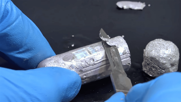
It looks like a tube made of glass but it’s actually aluminum. Well, aluminum with an asterisk beside it — this is not elemental aluminum but rather a material made using it.

We got onto the buzz about “transparent aluminum” as a result of a Tweet from whence the image above came. This Tweet was posted by [Jo Pitesky], a Science Systems Engineer at the Jet Propulsion Lab in Pasadena. [Jo] reported that at a recent JPL technology open house she had the chance to handle a tube of material that looks for all the world like a section of glass tubing, but was billed as transparent aluminum. [Jo] tweeted this because it was an interesting artifact that few people get to play with and she’s right, this is fascinating!

The the material itself is intriguing, and I immediately had practical questions like what is this stuff? What is it good for? How is it made? And is it really aluminum rendered transparent by some science fiction process?

Continue reading “What’s The Deal With Transparent Aluminum?”

Reverse Engineering Bottle Threads For Fun And Profit

Recently, one of [Eric]’s clients asked him to design a bottle. Simple enough for a product designer, except that the client needed it to thread into a specific type of cap. And no, they don’t know the specs.

But that’s no problem, thought [Eric] as he turned on the exhaust fan and reached for the secret ingredient that would make casting the negative image of the threads a breeze. He mixed up the foul-smelling body filler with the requisite hardener and some lovely cyan toner powder and packed it into the cap with a tongue depressor. Then he capped off the cast by adding a small PVC collar to lengthen the cast so he has something to grab on to when it’s time to take it out.

Bondo does seem like a good choice for casting threads. You need something workable enough to twist out of there without breaking, but rigid enough that the small detail of the threads isn’t lost. For the release agent, [Eric] used Johnson’s Paste Wax. He notes from experience that it works particularly well with Bondo, and even seems to help it cure.

Once the Bondo hardened, [Eric] made sure it screwed in and out of the cap and then moved on to CAD modeling and 3D printing bottle prototypes until he was satisfied. We’ve got the video screwed in after the break to cap things off.

Did you know that you can also use toner powder to tint your epoxy resin? Just remember that it is particulate matter, and take precautions.

Continue reading “Reverse Engineering Bottle Threads For Fun And Profit”