A modern recreation of von Guericke's electrostatic generator

Electrostatic Generator Project Starts With Molten Sulfur

Although the basic concept of electrostatic attraction has been known since ancient times, it was only in the 17th century that scientists began to systematically investigate electrostatics. One of the first to explore this new field was Otto von Guericke, who constructed an electrostatic generator to help with his experiments. [Markus Bindhammer] has reconstructed this machine, which formed the basis for later work by the likes of Wimshurst and Van de Graaff. [Markus] kept his machine in an almost period-correct fashion.

Von Guericke’s machine consists of a sulfur ball mounted on a spindle that allows it to be rotated and rubbed against a piece of cloth. By doing so, the ball gains a charge that can be used to attract small pieces of material. [Markus] built a neat wooden frame with faux-antique carved legs and installed a handle, a spindle, and a belt-drive system to rotate whatever’s mounted on the spindle at high speed.

A round-bottom flask containing sulfur being heated in an oil bathAll of this is beautifully documented in [Markus]’s video, but by far the most interesting part of his project is the process of manufacturing the sulfur ball. If you’ve always wanted one, here’s how to make one: first, melt some pieces of pure sulfur in a round-bottom flask using an oil bath. Then, turn on your vacuum pump to remove any air or water vapor trapped inside the liquid. Once the liquid is nice and clear, let it cool down and solidify very slowly; the sulfur ball can then be released from its container by breaking the glass with a hammer.

While it sounds simple, we can imagine it took a bit of experimenting to get all those steps just right. The end result is a simple but useful machine to demonstrate basic electrostatics, which [Markus] is planning to use in science lectures. There are lots of interesting experiments you can do with static electricity, including building a basic motor.

Continue reading “Electrostatic Generator Project Starts With Molten Sulfur”

A homebrew machine that dips a piece of wire into an etching solution

Homebrew Probe Tip Etcher Makes Amazingly Sharp Needles

There’s a simple reason why high-tech gadgets like PCs, TVs and smartphones are so cheap: they’re mass-produced. By spreading out huge engineering costs over equally huge production volumes, the cost per item can remain quite low. The flipside to this is that devices with only a small niche market can be extremely expensive even when they seem quite simple.

[Baird Bankovic], an undergrad student at Penn State University, discovered this when he was working with a scanning tunneling microscope (STM). He noticed that the machines used to make STM probes, a pretty straightforward process, cost north of $7500. This inspired him to make a cheap STM probe etching machine using simple homebrew parts.

If you’re not familiar with scanning tunneling microscopy, here’s how it works in a nutshell: a very sharp tungsten needle is positioned a few nanometers above the sample to be analyzed, and a small voltage is applied between the two. Through an effect known as quantum tunneling, a small current then flows between the probe and the sample. By observing this current and scanning the probe across the sample, a three-dimensional picture of the surface is obtained with sub-nanometer-level resolution.

One of the many factors that determine the quality of the image is the sharpness of the probe. Because a very sharp probe is extremely fragile and prone to oxidation, they are typically made on-site by dipping a piece of tungsten wire into an etchant in one of those costly machines.

That’s exactly what [Baird]’s device does: a Petri dish on a 3D printed frame holds a volume of sodium hydroxide solution, while a jackscrew Z-stage moves a probe holder up and down. A piece of tungsten wire is dipped into the solution and a voltage is applied to start the etching process. Because most of the etching happens at the liquid’s surface, the wire gets progressively thinner at that point until it snaps and the bottom half drops off. When this happens, the current through the wire changes rapidly, which triggers the machine to pull the wire out of the solution and stop the etching process.

The resulting probes have a well-defined sharp tip with an estimated width of about 50 nanometers — pretty impressive for such a simple setup. The entire hardware design is open source and available on [Baird]’s GitHub page for anyone to replicate. Nanometer-sized needles might only seem useful for those with a professional STM setup, but they also come in handy for all kinds of homebrew atomic-scale imaging experiments.

Continue reading “Homebrew Probe Tip Etcher Makes Amazingly Sharp Needles”

Zinc-Air, The Next Contender In Vehicle Batteries?

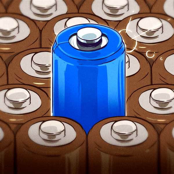
If you’ve got an interest in technology, it’s inevitable that your feed will feature a constant supply of stories with titles in the vein of “New battery breakthrough offers unlimited life and capacity!”. If we had a pound, dollar, or Euro for each one, we’d be millionaires by now. But while the real science behind the breathless headlines will undoubtedly have provided incremental battery improvements, we’re still waiting for the unlimited battery.

It’s not to say that they don’t conceal some interesting stories though, and there’s an announcement from Australia proving this point admirably. Scientists at ECU in Perth have created a new cathode compound for rechargeable zinc-air batteries, which it is hoped will make them much safer and cheaper competitors for lithium-ion cells.

Most of us think of zinc-air batteries as the tiny cells you’d put in a camera or a hearing aid, but these conceal a chemistry with significant potential that is held back by the difficulty of creating a reliable cathode. In these batteries the cathode is a porous support in which a reaction between zinc powder wet paste and oxygen in the air occurs, turning zinc into zinc oxide and releasing electrons which can be harvested as electricity. They have a very high power density, but previous cathode materials have quickly degraded performance when presented with significant load.

The new cathode support is a nano-composite material containing cobalt, nickel, and iron, and is claimed to offer much better performance without the degradation. Whether or not it can be mass-produced remains to be seen, but as a possible alternative to lithium-ion in portable and transport applications it’s of great interest.

Growing Oxides On Silicon On The Road To DIY Semiconductors

Doing anything that requires measurements in nanometers is pretty difficult, and seems like it would require some pretty sophisticated equipment. But when the task at hand is growing oxide layers on silicon chips in preparation for making your own integrated circuits, it turns out that the old Mark 1 eyeball is all you need.

Alert readers may recall that [ProjectsInFlight] teased this process in his previous video, which covered the design and construction of a DIY tube furnace. In case you missed that, a tube furnace is basically a long, fused quartz tube wrapped in electrical heating elements and lots of insulation, which is designed to reach the very high temperatures needed when making integrated circuits. The tube furnace proved itself up to the task by creating a thin layer of silicon dioxide on a scrap of silicon wafer. Continue reading “Growing Oxides On Silicon On The Road To DIY Semiconductors”

Copper Be Gone: The Chemistry Behind PCB Etching

For a lot of reasons, home etching of PCBs is somewhat of a dying art. The main reason is the rise of quick-turn PCB fabrication services, of course; when you can send your Gerbers off and receive back a box with a dozen or so professionally made PCBs for a couple of bucks, why would you want to mess with etching your own?

Convenience and cost aside, there are a ton of valid reasons to spin up your own boards, ranging from not having to wait for shipping to just wanting to control the process yourself. Whichever camp you’re in, though, it pays to know what’s going on when your plain copper-clad board, adorned with your precious artwork, slips into the etching tank and becomes a printed circuit board. What exactly is going on in there to remove the copper? And how does the etching method affect the final product? Let’s take a look at a few of the more popular etching methods to understand the chemistry behind your boards.

Continue reading “Copper Be Gone: The Chemistry Behind PCB Etching”

Supremely-tough Glass Performs Under Pressure

There’s some nifty research from the University of Bayreuth, together with partners in China and the U.S., on creating supremely tough aluminosilicate glass that boasts an unusual structure. The image above represents regular glass structure on the left, and the paracrystalline structure on the right.

Aluminosilicate, which contains silicon, aluminum, boron and oxygen, is a type of oxide glass. Oxide glasses are a group to which borosilicate and other common glasses belong. Structurally speaking, these glasses all have a relatively disordered internal structure. They’re known for their clarity, but not especially their durability. Continue reading “Supremely-tough Glass Performs Under Pressure”

Different Etching Strokes For Different PCBs, Folks

[Sebastian] probably didn’t think he was wading into controversial waters when he posted on his experimental method for etching PCBs (in German). It’s not like etching with hydrochloric acid and peroxide is anything new, really; it was just something new to him. But is it even possible these days to post something and not find out just how wrong you are about it?

Sadly, no, or at least so it appears from a scan of [Sebastian]’s tweet on the subject (Nitter). There are a bunch of ways to etch copper off boards, including the messy old standby etchant ferric chloride, or even [Sebastian]’s preferred sodium persulfate method. Being out of that etchant, he decided to give the acid-peroxide method a go and was much pleased by the results. The traces were nice and sharp, the total etching time was low, and the etchant seemed pretty gentle when it accidentally got on his skin. Sounds like a win all around.

But Twitter wouldn’t stand for this chemical heresy, with comments suggesting that the etching process would release chlorine gas, or that ferric chloride is far safer and cleaner. It seems to us that most of the naysayers are somewhat overwrought in their criticism, especially since [Sebastian]’s method used very dilute solutions: a 30% hydrochloric acid solution added to water — like you oughta — to bring it down to 8%, and a 12% peroxide solution. Yes, that’s four times more concentrated than the drug store stuff, but it’s not likely to get you put on a terrorism watch list, as some wag suggested — a hair stylist watchlist, perhaps. And 8% HCl is about the same concentration as vinegar; true, HCl dissociates almost completely, which makes it a strong acid compared to acetic acid, but at that dilution it seems unlikely that World War I-levels of chlorine gas will be sweeping across your bench.

As with all things, one must employ caution and common sense. PPE is essential, good chemical hygiene is a must, and safe disposal of spent solutions is critical. But taking someone to task for using what he had on hand to etch a quick PCB seems foolish — we all have our ways, but that doesn’t mean everyone else is wrong if they don’t do the same.

Continue reading “Different Etching Strokes For Different PCBs, Folks”