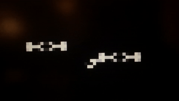
We’re not sure what the assignment was, but the results of [Garret Carter]’s homework for his Digital System Design class at Tennessee Tech couldn’t help but capture our attention. Below the break you can see what [Garrett] describes as a “simplified stylized version” of the 1981 arcade hit “Defender”.
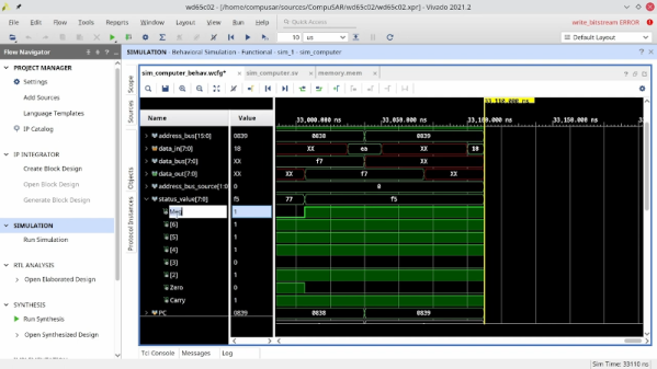
With the goal of keeping the price low but keeping performance as high as possible, [Garrett] set forth to program the DE10-Lite FPGA development board in VHDL. The results are convincing, and while not perfect, came in under budget.
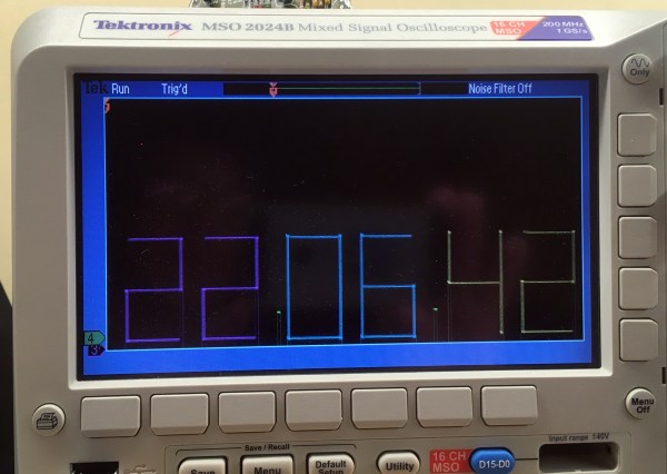
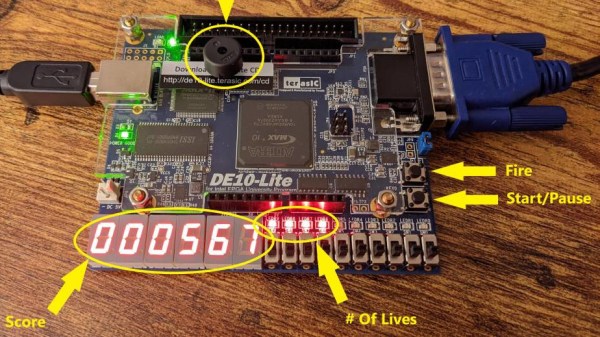
The DE10-Lite board gave [Garrett] the opportunity to get even more creative, using the dev board’s onboard switches, buttons, 7-segment LED’s and accelerometer to full effect. In this case, the dev board is not only the game, but also the controller and status display. A very neat hack indeed!
If you want to make your own, you can get the full project details at [Garrett]’s Github page. And [Garrett], we don’t know what marks your professor will give, but we give you an A+, would definitely play again.
While FPGA development boards aren’t necessarily inexpensive, our own Jenny List shows where you might be able to find a used but workable FPGA board for a fraction of the cost, If you know where to look.
Continue reading “DE10-Lite-Ful FPGA Dev Board Hack Plays The 1981 Classic Defender”