Xilinx Borrows Code For Their Own Devices

Back in 2012, [tmbinc] discovered a neat little undocumented feature in the Xilinx ISE: the ability to use TCP/IP instead of JTAG cables. [tmbinc] was working on an Open Hardware USB analyzer and discovered the nearly undocumented Xilinx Virtual Cable, a single ‘shift’ command that opens up a TCP connection and sends JTAG data out to another computer on the network. It’s extraordinarily useful, [tmbinc] wrote a daemon for this tool, and everything was right with the world.

Yesterday, [tmbinc] discovered the Xilinx Virtual Cable again, this time in one of Xilinx’s Github repos. The code was extraordinarily familiar, and looking closer at a few of the revisions, he saw it was very similar to code he had written three years ago.

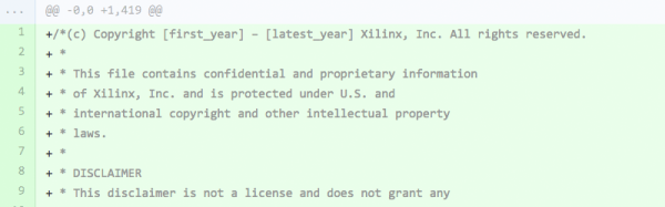
The offending revision in the Xilinx repo is nearly identical to [tmbinc]’s Xilinx Virtual Cable Driver daemon. Variable names are the same, the variables are declared in the same order, and apart from whitespace, code conventions are the same. This is not to say someone at Xilinx stole code from [tmbinc], but if this were a computer science lab, there would be an academic disciplinary hearing. What’s worse, Xilinx plastered their copyright notice at the top of the code.

In an issue [tmbinc] raised, he said he was flattered, but clarified that his code was developed entirely from scratch. He believes the Xilinx code was derived from his own code written three years ago. Since [tmbinc]’s code was uploaded without a license, it defaulted to All Rights Reserved. This does not bode well for the Xilinx legal department.

In any event, you really, really have to wonder what Xilinx’s internal documentation looks like if a random person on the Internet can discover a barely-documented protocol, write a daemon, put it on the Internet, and have someone at Xilinx use that code.

Thanks to the anonymous tipster for sending this into the Hackaday tip jar.
FPGA Based Ambilight Clone

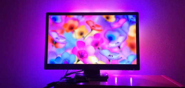
The Philips Ambilight – a bunch of rear-facing RGB LEDs taped to the back of a TV – is becoming the standard project for anyone beginning to tinker with FPGAs. [DrX]’s is the best one we’ve seen yet, with a single board that reads and HDMI stream, makes blinkey lights go, and outputs the HDMI stream to the TV or monitor.

[DrX] is using an FPGA development board with two HDMI connectors – the Scarab miniSpartan6+ – and a strand of WS2801 individually addressable RGB LEDs for this project. With a bit of level shifting, driving the LEDs was easily taken care of. But what about decoding HDMI?

Most of the project is borrowed from a project that displays a logo in the corner of a 720p video stream. The hardware is the same, but for an Ambilight clone, you need to read the video stream and process it, not just write to it. By carefully keeping track of the R, G, and B values for each pixel along with the pixel clock,  the colors along the edge of a display can be averaged. It’s not as difficult or as memory-intensive as building a frame buffer; nearly all of the picture data is thrown out when assembling the averages around the perimeter of the display. It does work, though.

After figuring out the average color around the perimeter of the display, it’s just a simple matter of driving the LEDs. Tape those LEDs to the back of a TV, and there’s an Ambilight clone, made with an FPGA.

[DrX] has a few videos of his project in action. You can check those out below.

Continue reading “FPGA Based Ambilight Clone” →

VCF East X: The World’s Largest USB Thumb Drive

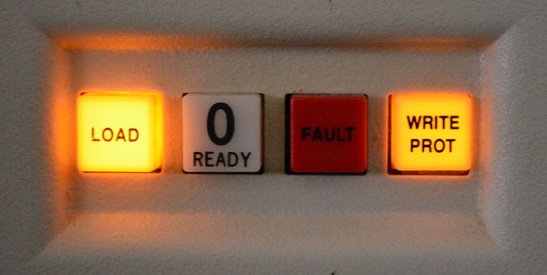
The Vintage Computer Festival last weekend featured racks and racks of old minicomputers, enough terminals for an entire lab, and enough ancient storage devices to save a YouTube video. These storage devices – hard disks, tape readers, and 8″ disk drives – were only connected to vintage hardware, with one exception: a DEC RL02 drive connected to a modern laptop via USB.

The DEC RL02 drive is the closest you’re going to get to a modern mechanical hard drive with these old machines. It’s a huge rack unit with removable platters that can hold 10 Megabytes of storage. [Chris] found one of these old drives and because he wanted to get into FPGA development, decided to create a USB adapter for this huge, old drive.

The hardware isn’t too terribly complex, with a microcontroller and an FPGA that exposes the contents of the drive over USB mass storage. For anyone trying to bootstrap a PDP-11 or -8 system, [Chris] could download disk images from the Internet, write them to the disk, and load up the contents of the drive from the minicomputer. Now, he’s using it with SimH to have a physical drive for an emulated system, but the controller really doesn’t care about what format the disk pack is in. If [Chris] formatted a disk pack with a FAT file system, he would have the world’s largest and heaviest USB thumb drive in the world.

Video below.

Update: As promised, [Chris] put all the code in a git

Continue reading “VCF East X: The World’s Largest USB Thumb Drive” →

Reverse Engineering Lattice’s ICE40 FPGA Bitstream

Unlike microcontroller projects, projects involving FPGAs cannot yet claim to rely on a mature open-source toolchain. Each FPGA will, at some point, need to be configured with a proprietary bitstream produced from a closed source synthesis tool. This lack of a full FPGA toolchain to take your project from Verilog-or-VHDL to an uploadable bitstream is due to many reasons. First, writing such a “compiler” is complicated. It involves intimate knowledge of the resources available on the FPGA that can assimilate the functionality of the intended design. Second, the entire synthesis procedure is closed-source, a “secret sauce” of sorts for each FPGA vendor.

In response, [Alex] and [Clifford] have taken the first step towards an open-source toolchain for one FPGA; they’ve reverse-engineered the bitstream of Latttice Semiconductor’s iCE40 FPGA. The duo didn’t just pick the iCE40 on a whim. This choice was deliberately because that FPGA is available on a development board for a mere $22 so that others could follow in their footsteps without breaking the bank.

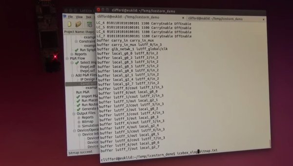
In the video below, [Clifford] demos the functionality of this new tool by synthesizing a design from Verilog to a bitstream and then back from a bitstream to Verilog. Given this feature, a staggering amount of work has been done towards developing a polished open-source toolchain for this particular FGPA.

To snag a copy of the latest code, have a look at its documentation page.

Continue reading “Reverse Engineering Lattice’s ICE40 FPGA Bitstream” →

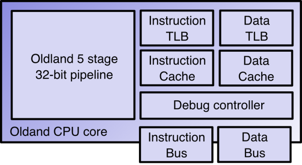
A block diagram of the Oldland CPU core

The Oldland CPU 32-bit FPGA Core

Field Programmable Gate Arrays (FPGAs) let you program any logic you’d like onto a chip. You write your logic using a hardware description language, then flash it to the FPGA. You can even design your own processor and flash it to the chip.

That’s exactly what [jamieiles] has done with the Oldland CPU. It’s an open source 32 bit CPU core that you can synthesize for use on an FPGA. Not only can you browse through all the Verilog code in the Github repo, but there’s also a bunch of tools for working with this CPU core.

Included with the package is oldland-rtlsim, which lets you simulate the processor on a PC. The oldland-debug tool lets you connect to the processor for programming and debugging over JTAG. Finally, there’s a GNU toolchain port that lets you build C code for the device.

Going one step futher, [jamieiles] built a full SoC around the Oldland core. This has SPI, UART, timers, and more features you’d expect to find in a microcontroller. It can be flashed to the relatively cheap Terasic DE0-Nano board.

[jamieiles] has also ported u-boot to the processor, and the next thing on the list is the Linux kernel. If you’ve ever been interested in how CPUs actually work, this is a neat project to look through. If you want more open source CPU cores, check out OpenCores.

Using The Red Pitaya As An SDR

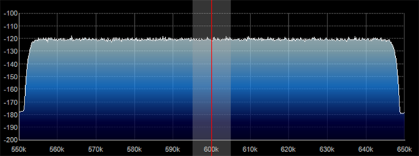
The Red Pitaya is a credit-card sized board that runs Linux, has Ethernet, and a good bit of RAM. This sounds a lot like a Raspberry Pi and BeagleBone Black, but the similarities end there. The Red Pitaya also has two RF inputs, two RF outputs, and a load of digital IOs, all connected to an Xilinx SoC that includes an FPGA. [Pavel] realized the Pitaya had all the components of a software-defined radio, and built an implementation to prove it.

The input for the SDR taps directly into one of the high impedance inputs with a simple loop antenna made out of telephone cable. The actual software-defined part of this radio borrows heavily from an Xilinx application note, while everything is controlled by either SDR# or HDSDR.

[Pavel] included a pre-built SD card image with all his software, so cloning this project is simply a matter of copying an SD card and building an antenna. The full source is also available, interesting if you would like to muck about with FPGAs and SDRs.

HDMI Audio And Video For Neo Geo MVS

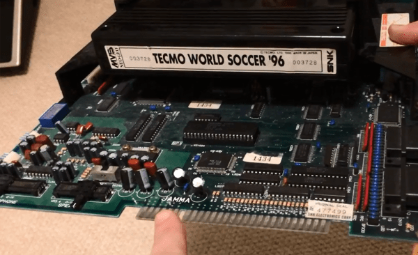
[Charlie] was killing some time hacking on some cheap FPGA dev boards he bought from eBay. Initially, he intended to use them to create HDMI ports for a different project before new inspiration hit him. Instead, he added an HDMI port to Neo Geo MVS games. The Neo Geo MVS was a 90’s arcade machine that played gems like the Metal Slug and Samurai Showdown series. [Charlie] has a special knack for mods, being featured on Hackaday before for implementing Zork on hardware and making a mini supergun PCB. What’s especially nice about his newest mod is that the HDMI outputs both audio and video.

[Charlie] obtained the best possible video and audio signal by tapping the digital inputs to the Neo Geo’s DACs (digital-to-analog converter). The FPGA was then used to convert the signals to HDMI, maintaining a digital signal path from video generation to display. While this sounds simple enough, there was a lot that had to be done. The JAMMA video standard’s lower resolution was incompatible with the various resolutions offered by the HDMI protocol. [Charlie] solved this problem by implementing scan doubling using the RAM on the Cyclone II dev board. He then had to downsample the audio to 32kHz (from 55.6kHz) in order to meet the HDMI specs. Getting the sound over HDMI required adding data islands to the signal, a feat [Charlie] admits was a frustrating one.

When he tested the HDMI with his monitor, it was out of spec but still worked. His TV, on the other hand, refused to play it at all. This was due to the Neo Geo outputting 59.1 fps – not the standard 60 fps. Using the FPGA, [Charlie] overclocked the NeoGeo by approximately 1% and used the 27Mhz pixel clock to change the FPGA output to a 720 x 480p signal.

For those that love the scan lines of yore, they can be enabled with the push of a button. [Charlie] notes that there are some slight differences in the shadow effects of some graphics, but he has done his best to minimize them. He also admits that the FPGA code contributes only 100 microseconds of delay compared to analog output, which is fast enough for even the most hardcore gamers.

Check out the video after the break to see how the Neo Geo looks in HDMI along with a side-by-side comparison to a CRT TV.

Continue reading “HDMI Audio And Video For Neo Geo MVS” →