Visualizing Ionizing Radiation With DIY Plastic Scintillators

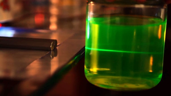
Although most types of radiation are invisible, except for the visible part of the EM spectrum, there are many ways that we can make various types of radiation visible. One of these methods is called ‘scintillation’, which can be used to make ionizing radiation visible. Recently [Lukas Springer] demonstrated how to make scintillators out of what is essentially plastic: bisphenol-A (E45, ‘epoxy’) resin with hardener and other additives.

The essential principle of operation behind a scintillator is its sensitivity to ionizing radiation, along with the tendency to absorb the energy and re-emit it in the form of light, i.e. luminescence. This is akin to the luminescence of LEDs, except that in their case the underlying principle is that of electro-luminescence. In the case of a plastic scintillator, the scintillating material is suspended in the solid polymer matrix base.

As [Lukas] points out, plastic scintillators are hardly ideal when it comes to their sensitivity to ionizing radiation, but they compensate for this by being easy to shape and produce, while being very durable. For this experiment, he used regular epoxy as the scintillator matrix, p-Terphenyl as primary scintillator and Coumarin 102 as the wavelength shifter. These three compounds act as a reaction chain, with the matrix absorbing the radiation and transferring it to the primary scintillator, which in turns emits the energy as light.

As the primary scintillator tends to radiate in the deep UV part of the EM spectrum, a wavelength shifter (i.e. secondary scintillator) which ‘shifts’ the emitted UV radiation into the visible part of the spectrum.

After producing a batch of plastic scintillators following the above recipe, [Lukas] irradiated them with gamma radiation, and found them to perform worse than some already not remarkable Russian PS-based scintillators. [Lukas’s] guess is that the matrix may be absorbing the primary scintillator’s output, or a mismatch between the primary and second scintillator.

While tricky to get right, it does seem like a fun hobby if one has some interesting in chemistry. [Lukas] (@GigaBecquerel on Twitter) provides a basic recipe as well as many other compounds to use for the primary and secondary scintillator, as well as the matrix compound. Enough to get started with.

Growing Opals In The Lab

Opals are unique amongst gemstones, being formed from tiny silica nanospheres arranged in precise structures that give them their characteristic shifting color when seen from different angles. [The Thought Emporium] loves a challenge, so set about growing some himself.

It’s not the hardest gemstone synthesis ever, but it’s no cakewalk either. The process requires tetraethyl orthosilicate, or TEOS, which can be difficult to find, but the rest of the chemicals required are commonly available. The initial phase involves mixing the TEOS with reactants to form nanoscale silica spheres in the range of 200-350 nanometers wide. With the spheres in solution, the mixture must then be carefully dried in such a way as to create the right structure to produce opal’s famous color effects. At this stage, industrial producers add further silica to stabilize the matrix, though [The Thought Emporium] wasn’t able to find literature that explained how to do this. Instead, he relied on resin, which while imperfect, did allow the specimens to be stabilised and shown off for the purposes of the video.

The video notes that many of the steps in this process were perfected decades ago, but remain held as trade secrets, making replication an exercise in experimentation. Nonetheless, success was had in producing recognisably opalescent specimens, and we can’t wait to see further refinement of the DIY process.

We’ve seen similar work from [The Thought Emporium] before, exploring structural color and holograms. Video after the break.

Continue reading “Growing Opals In The Lab”

Active Camouflage Material Shows Promise At Hiding From Infrared Or Visual Detection

An invisibility cloak may seem like science fiction, but despite that, many scientists and engineers have put much time into developing the concept, pushing it closer to reality. A device which detects the nature of its surroundings and changes its own properties to blend in may be complex, but a multitude of examples in the animal world show that it’s not impossible to achieve.

A team from Seoul National University recently developed a flexible material designed in part as a flexible “cloaking” material. We’ll take a look at the underlying concept behind such devices below, and look at how this work furthers the state of the art in the field.

Continue reading “Active Camouflage Material Shows Promise At Hiding From Infrared Or Visual Detection”

Xolography: A Method To Improve The Accuracy Of Volumetric 3D Printing

Over the past years, additive manufacturing (AM) has become a common tool for hackers and makers, with first FDM and now SLA 3D printers becoming affordable for the masses. While these machines are incredibly useful, they utilize a slow layer-by-layer approach to produce objects. A relatively new technology called Volumetric Additive Manufacturing (VAM) promises to change all that by printing the entire object in one go, and according to a recent article in Nature, it just got a big resolution boost.

The concept is similar to SLA printing, but instead of curing the resin by projecting a 2D image of the current layer into the container, VAM uses multiple lasers to create intersecting points within the liquid. After exposing the resin to this projection for several seconds, the 3D model is built all at once. Not only is this far faster, but it removes the need for support materials and even a traditional build plate is unnecessary.

Visualization of the dual-color printing process as used by Regehly et al. (Credit: Nature)

Up till now the resolution and maximum object size of VAM has left a lot to be desired, but in this new research by Regehly et al. claim to have accomplished a feature resolution of ‘up to 25 micrometers’ and a solidification rate of ‘up to 55 cm3/s’. They used two crossing laser beams of different wavelengths, one to form the ‘light sheet’ (blue in the graphic) and a second beam (in red) to project the slide onto this light sheet. They refer to this technique as ‘xolography’, as a mesh-up of ‘holo’ (Greek for ‘whole’) and the ‘X’ shape formed by the crossing laser beams.

Key to making this work is the chemistry of the resin: the first wavelength excites the molecules called DCPI (Dual-Color Photo Initiators) that are dissolved in the resin. The second wavelength when hitting the same molecules initiates the resin polymerization process. The object pictured at the top of the page was a test print; producing such a design on a traditional 3D printer would have required a considerable amount of difficult to remove support material.

While this is obviously not a technology hobbyists will be using to replace their FDM and SLA printers with any time soon, there are still many companies and institutes working on various VAM technologies and approaches. As more and more of the complexities and challenges are dealt with, who knows when VAM may become a viable replacement for at least some SLA applications?

Thanks to [Qes] for the tip.

How A Quadriplegic Patient Was Able To Eat By Himself Again Using Artificial Limbs

Thirty years ago, [Robert “Buz” Chmielewski] suffered a surfing accident as a teenager. This left him as a quadriplegic due to a C6 spinal cord injury. After becoming a participant in a brain-computer interface study at Johns Hopkins, he was recently able to feed himself through the use of prosthetic arms. The most remarkable thing about these prosthetic arms is primarily the neural link with [Buz’s] brain, which allows him to not only control the artificial arms, but also feel what they are touching, due to a closed-loop system which transfers limb sensory input to the patient’s brain.

The prosthetic limb in question is the Modular Prosthetic Limb (MPL) from Johns Hopkins Applied Physics Laboratory (APL). The Johns Hopkins Medicine Brain-Computer Interface study began a year ago, when [Buz] had six microelectrode arrays (MEA) implanted into his brain: half in the motor cortex and half in the sensory cortex. During the following months, the study focused on using the signals from the first set of arrays to control actuators, such as the MPL. The second set of arrays was used to study how the sensory cortex had to be stimulated to allow a patient to feel the artificial limb much as one feels a biological limb.

What makes this study so interesting is not only the closed-loop approach which provides the patient with feedback on the position and pressure on the prosthetic, but also that it involves both hemispheres of the brain. As a result, after only a year of the study, [Buz] was able to use two of the MPLs simultaneously to feed himself, which is a delicate and complicated tasks.

In the video embedded after the break one can see a comparison of [Buz] at the beginning of the study and today, as he manages to handle cutlery and eat cake, without assistance.

Continue reading “How A Quadriplegic Patient Was Able To Eat By Himself Again Using Artificial Limbs”

LEDs-On-Chips Will Give Us Lower Cost Optoelectronics

The LED is one of those fundamental building block components in electronics, something that’s been in the parts bin for decades. But while a simple LED costs pennies, that WS2812 or other fancy device is a bit expensive because internally it’s a hybrid of a silicon controller chip and several LEDs made from other semiconductor elements. Incorporating an LED on the same chip as its controller has remained something of a Holy Grail, and now an MIT team appear to have cracked it by demonstrating a CMOS device that integrates a practical silicon LED. It may not yet be ready for market but it already displays some interesting properties such as a very fast switching speed. Perhaps more importantly, further integration of what have traditionally been discrete components would have a huge impact on reducing manufacturing costs.

Anyone who has read up on the early history of LEDs will know that the path from the early-20th-century discoveries of semiconductor luminescence through the early commercial devices of the 1960s and up to the bright multi-hued devices of today has been a long one with many stages of the technology reaching the market. Thus these early experimental silicon LEDs produce light in the infrared spectrum often useful in producing sensors. Whether we’ll see an all-silicon Neopixel any time soon remains to be seen, but we can imagine that some sensors using LEDs could be incorporated on the same die as a microcontroller. It seems there’s plenty of potential for this invention.

This research was presented earlier this month at the IEDM Conference in a talk entitled Low Voltage, High Brightness CMOS LEDs. We were not able to find a published paper, we’d love read deeper so let us know in the comments below if you have info on when this will become available. In the meantime, anyone with any interest in LED technology should read about Oleg Losev, the inventor of the first practical LEDs.

Magnetocuring: Curing Epoxy With A Magnetic Field

Who doesn’t love epoxy? Epoxy resins, also known as polyepoxides, are an essential adhesive in many applications, both industrially and at smaller scales. Many polyepoxides however require the application of heat (around 150 °C for most types) in order to cure (harden), which can be complicated when the resin is applied to or inside layers of temperature sensitive materials. Now researchers at Nanyang Technological University (NTU) in Singapore have found a way to heat up resins using an alternating magnetic field (PDF), so-called magnetocuring.

As detailed in the research article by R. Chaudhary et al., they used commercially available epoxy resin and added nano particles of a MnxZn1-xFe2O4 alloy. This mixture was exposed to an alternating magnetic field to induce currents in the nano particles and subsequently produce heat that served to raise the temperature of the surrounding resin to about 160 °C in five minutes, allowing the resin to cure. There is no risk of overheating, as the nano particles are engineered to reach their Curie temperature, at which point the magnetic field no longer affects them. The exact Curie temperature was tweaked by changing the amount of manganese and zinc in the alloy.

After trying out a number of different alloy formulations, they settled on Mn0.7Zn0.3Fe2O4 as the optimal formulation at which no resin scorching occurred. As with all research it’s hard to tell when (and if) it will make it into commercial applications, but if this type of technology works out we could soon be gluing parts together using epoxy resin and an EM field instead of fumbling with the joys of two-component epoxy.

(Thanks, Qes)