Mining projects are approved or disapproved based on all kinds of reasons. There are economic concerns, logistical matters, and environmental considerations to be made. Mining operations can be highly polluting, or they can have outsized effects on a given area by sheer virtue of the material they remove or the byproducts they leave behind.
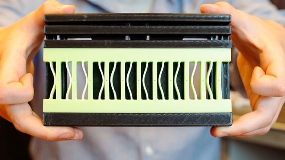
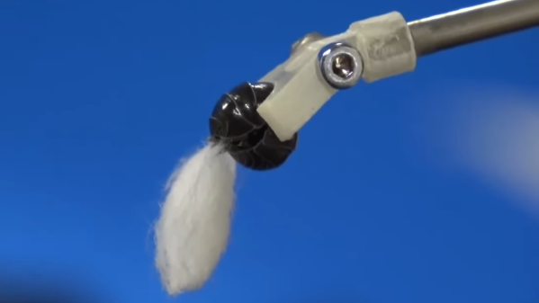
The block contains beams, and by controlling how the block is compressed, the vertical beams shift in a stable and consistent way, acting as a mechanical counter. It’s a straightforward implementation of the work of two physicists from the Netherlands: [Martin van Hecke] and [Lennard Kwakernaak].
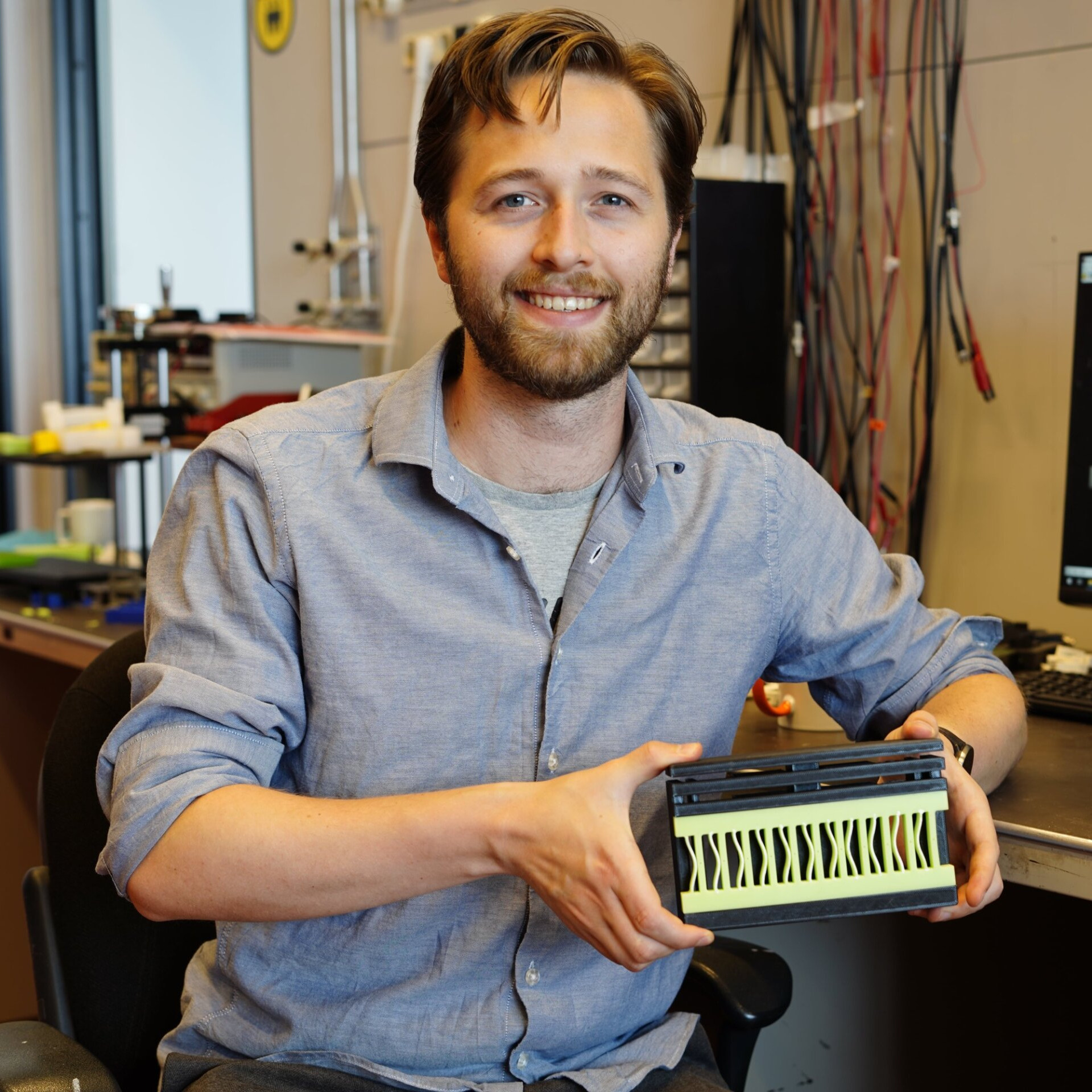
You can check out the research paper for more details on the rubber beam counter. [Kwakernaak] aims to create a much more complex structure with elements that interact across a plane instead of in a single direction. Such a device would, in effect, be a simple computer.
Watch the beam counter in action in the short video embedded below. See how the elements of the green rubber block move while constrained by an outer frame that helps control the force that is applied. The thin beams flip from left to right, one at a time with each press.
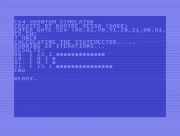
The term ‘quantum computer’ gets usually tossed around in the context of hyper-advanced, state-of-the-art computing devices. But much as how a 19th century mechanical computer, a discrete computer created from individual transistors, and a human being are all computers, the important quantifier is how fast and accurate the system is at the task. This is demonstrated succinctly by [Davide ‘dakk’ Gessa] with 200 lines of BASIC code on a Commodore 64 (GitHub), implementing a range of quantum gates.
Much like a transistor in classical computing, the qubit forms the core of quantum computing, and we have known for a long time that a qubit can be simulated, even on something as mundane as an 8-bit MPU. Ergo [Davide]’s simulations of various quantum gates on a C64, ranging from Pauli-X, Pauli-Y, Pauli-Z, Hadamard, CNOT and SWAP, all using a two-qubit system running on a system that first saw the light of day in the early 1980s.
Naturally, the practical use of simulating a two-qubit system on a general-purpose MPU running at a blistering ~1 MHz is quite limited, but as a teaching tool it’s incredibly accessible and a fun way to introduce people to the world of quantum computing.
[NightHawkInLight] has been working on radiative sky paint. (Video, embedded below.) That’s a coating that radiates heat in the infrared spectrum at a wavelength that isn’t readily absorbed or reflected by the atmosphere. The result is a passive system that keeps materials a few degrees cooler in direct sunlight than an untreated piece in the shade. That sounds a bit like magic, but apparently the math checks out.
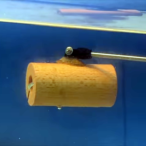
A research paper titled Biological Organisms as End Effectors explores the oddball approach of giving small animals jobs as grippers at the end of a robotic arm. Researchers show that pill bugs and chitons — small creatures with exoskeletons and reflexive movements — have behaviors making them useful as grippers, with no harm done to the creatures in the process. The prototypes are really just proofs of concept, but it’s a novel idea that does work in at least a simple way.
Pill bugs reflexively close, and in the process can grasp and hold lightweight objects. The release is simply a matter of time; researchers say that after about 115 seconds a held object is released naturally when the pill bug’s shell opens. While better control over release would be good, the tests show basic functionality is present.
The chiton — a small mollusk — can grip underwater.
Another test involves the chiton, a small mollusk that attaches to things with suction and can act as an underwater end effector in a similar way. Interestingly, a chiton is able to secure itself to wood and cork; materials that typical suction cups do not work on.
A chiton also demonstrates the ability to manipulate a gripped object’s orientation. Chitons seek dark areas, so by shining light researchers could control in which direction the creature attempts to “walk”, which manipulates the held object. A chiton’s grip is strong, but release was less predictable than with pill bugs. It seems chitons release an object more or less when they feel like it.
This concept may remind readers somewhat grimly of grippers made from dead spiders, but researchers emphasize that we have an imperative to not mistreat these living creatures, but to treat them carefully as we temporarily employ them in much the same manner as dog sleds or horses have been used for transportation, or carrier pigeons for messages. Short videos of both pill bug and chiton grippers are embedded below, just under the page break.
If you are a science fiction fan, you probably hate the theory of relativity. After all, how can the Enterprise get to a new star system every week if you can’t go faster than the speed of light? [Nick Lucid] wants to set you straight: it is real, and you can prove it to yourself for under $100.
The idea uses muons created in our atmosphere by cosmic rays colliding with gasses in the atmosphere. So how do you detect muons yourself? [Nick] shows you how to do it with a fish tank, dry ice, and rubbing alcohol. If that sounds like a cloud chamber, you aren’t wrong.
A cloud chamber is undeniably cool, but how does it prove relativity? You’ll see several kinds of particles interacting with your cloud chamber, but you can tell which ones are muons by the size and motion of the streaks. The muons don’t last very long. So you’d expect very few muons to make it to the surface of the Earth. But they not only reach the surface but go deep under it, as well.
So how do you explain it? Relatively. The muon experiences its average 2.2 microseconds lifetime in what appears to us to be over 150 microseconds, even if it is moving relatively slowly for a muon. Some muons are faster or live longer, so we see a lot of them hit the Earth every minute of every day. This is due to time dilation and also explains length contraction because the muon moves at a certain speed, yet it appears to go further to us than to the muon.
Coincidentally, we recently discussed this same effect relative to using muons for underground navigation. If you want an easier way to count muons with a computer, you can build a detector for about the same price as the cloud chamber.
Despite how hostile to life some parts of the Earth’s continents are, humanity has enthusiastically endeavored over the course of millennia to establish at least a toehold on each of them. Yet humanity has barely ventured beyond the surface of the oceans which cover around three-quarters of the planet, with human activity in these bodies of water dropping off quickly along with the fading of light from the surface.
Effectively, this means for all intents and purposes we have to this day not explored the vast majority of the Earth’s surface, due to over 70% of it being covered by water. As an ocean planet, much of Earth’s surface is covered by watery depths of multiple kilometers, with each 10 meters of water increasing the pressure by one atmosphere (1.013 bar), so that at a depth of one kilometer we’re talking about an intense 101 atmospheres.
Over the past decades, the 1985 discovery of Titanic’s wreck approximately 3.8 kilometer below the surface of the Atlantic, the two year long search for AF447’s black boxes, and the fruitless search for the wreckage of MH370 despite washed-up remnants have served as stark reminders of just how alien and how hostile the depths of the Earth’s oceans are. Yet with both tourism and mining efforts booming, will we one day conquer the full surface of Earth?