Your Own Open Source ASIC: SkyWater-PDK Plans First 130 Nm Wafer In 2020

You might have caught Maya Posch’s article about the first open-source ASIC tools from Google and SkyWater Technology. It envisions increased access to make custom chips — Application Specific Integrated Circuits — designed using open-source tools, and made real through existing chip fabrication facilities. My first thought? How much does it cost to tape out? That is, how do I take the design on my screen and get actual parts in my hands? I asked Google’s Tim Ansel to explain some more about the project’s goals and how I was going to get my parts.

The goals are pretty straightforward. Tim and his collaborators would like to see hardware open up in the same way software has. The model where teams of people build on each other’s work either in direct collaboration or indirectly has led to many very powerful pieces of software. Tim’s had some success getting people interested in FPGA development and helped produce open tools for doing so. Custom ASICs are the next logical step.

Continue reading “Your Own Open Source ASIC: SkyWater-PDK Plans First 130 Nm Wafer In 2020”

Creating A Custom ASIC With The First Open Source PDK

A process design kit (PDK) is a by now fairly standard part of any transformation of a new chip design into silicon. A PDK describes how a design maps to a foundry’s tools, which itself are described by a DRM, or design rule manual. The FOSSi foundation now reports on a new, open PDK project launched by Google and SkyWater Technology. Although the OpenPDK project has been around for a while, it is a closed and highly proprietary system, aimed at manufacturers and foundries.

The SkyWater Open Source PDK on Github is listed as a collaboration between Google and SkyWater Technology Foundry  to provide a fully open source PDK and related sources. This so that one can create manufacturable designs at the SkyWater foundry, that target the 130 nm node. Open tools here should mean a far lower cost of entry than is usually the case.

Although a quite old process node at this point (~19 years), it should nevertheless still be quite useful for a range of applications, especially those that merge digital and analog circuitry. SkyWater lists their SKY130 node technology stack as:

  • Support for internal 1.8V with 5.0V I/Os (operable at 2.5V)
  • 1 level of local interconnect
  • 5 levels of metal
  • Inductor-capable
  • High sheet rho poly resistor
  • Optional MiM capacitors
  • Includes SONOS shrunken cell
  • Supports 10V regulated supply
  • HV extended-drain NMOS and PMOS

It should be noted that use of this open source PDK is deemed experimental at this point in time, and should not be used for any commercial or otherwise sensitive applications.

Header image: Peellden/ CC BY-SA 3.0

Fail Of The Week: Bright Idea For LED Signs Goes Bad

Typically when we select a project for “Fail to the Week” honors, it’s because something went wrong with the technology of the project. But the tech of [Leo Fernekes]’ innovative LED sign system was never the problem; it was the realities of scaling up to production as well as the broken patent process that put a nail in this promising project’s coffin, which [Leo] sums up succinctly as “The Inventor’s Paradox” in the video below.

The idea [Leo] had a few years back was pretty smart. He noticed that there was no middle ground between cheap, pre-made LED signs and expensive programmable signboards, so he sought to fill the gap. The result was an ingenious “LED pin”, a tiny module with an RGB LED and a microcontroller along with a small number of support components. The big idea is that each pin would store its own part of a display-wide animation in flash memory. Each pin has two terminals that connect to metal cladding on either side of the board they attach to. These two conductors supply not only power but synchronization for all the pins with a low-frequency square wave. [Leo]’s method for programming the animations — using a light sensor on each pin to receive signals from a video projector — is perhaps even more ingenious than the pins themselves.

[Leo]’s idea seemed destined for greatness, but alas, the cruel realities of scaling up struck hard. Each prototype pin had a low part count, but to be manufactured economically, the entire BOM would have to be reduced to almost nothing. That means an ASIC, but the time and expense involved in tooling up for that were too much to bear. [Leo] has nothing good to say about the patent game, either, which his business partners in this venture insisted on playing. There’s plenty of detail in the video, but he sums it up with a pithy proclamation: “Patents suck.”

Watching this video, it’s hard not to feel sorry for [Leo] for all the time he spent getting the tech right only to have no feasible way to get a return on that investment. It’s a sobering tale for those of us who fancy ourselves to be inventors, and a cautionary tale about the perils of participating in a patent system that clearly operates for the benefit of the corporations rather than the solo inventor. It’s not impossible to win at this game, as our own [Bob Baddeley] shows us, but it is easy to fail.

Continue reading “Fail Of The Week: Bright Idea For LED Signs Goes Bad”

Weird World Of Microwaves Hack Chat

Join us on Wednesday, December 18 at noon Pacific for the Weird World of Microwaves Hack Chat with Shahriar Shahramian! We’ve been following him on The Signal Path for years and are excited to pick his brain on what is often considered one of the dark arts of electronics.

No matter how much you learn about electronics, there always seems to be another door to open. You think you know a thing or two once you learn about basic circuits, and then you discover RF circuits. Things start to get a little strange there, and stranger still as the wavelengths decrease and you start getting into the microwave bands. That’s where you see feed lines become waveguides, PCB traces act as components, and antennas that look more like musical instruments.

Shahriar is no stranger to this land. He’s been studying millimeter-wave systems for decades, and his day job is researching millimeter-wave ASICs for Nokia Bell Labs in New Jersey, the birthplace of the transistor. In his spare time, Shahriar runs The Signal Path, a popular blog and YouTube channel where he dives tear-downs, explanations, and repairs of incredibly sophisticated and often outrageously expensive equipment.

We’ll be sitting down with Shahriar this week for the last Hack Chat of 2019 with a peek inside his weird, wonderful world of microwaves. Join us with your questions about RF systems, microwaves in the communication industry, and perhaps even how he manages to find the gear featured on his channel.

join-hack-chatOur Hack Chats are live community events in the Hackaday.io Hack Chat group messaging. This week we’ll be sitting down on Wednesday, December 18 at 12:00 PM Pacific time. If time zones have got you down, we have a handy time zone converter.

Click that speech bubble to the right, and you’ll be taken directly to the Hack Chat group on Hackaday.io. You don’t have to wait until Wednesday; join whenever you want and you can see what the community is talking about.

Chisel Away At FPGA Development

Most of the time if you were to want to develop for an FPGA, you might turn to Verilog or VHDL. Both of these are quite capable, but they are also firmly rooted in languages that are old-fashioned by today’s standards. There have been quite a few attempts to treat those languages as an output to some other tool — either a higher-level language or a graphical tool. One recent effort is a toolchain that starts with Chisel.

The idea behind Chisel is to provide Scala with Verilog-like constructs. If you want, you can use it as a “super Verilog” taking advantage of classes and other features. However, Chisel also allows you to create generators that produce different output Verilog depending on how you call them. True, you can do some of this with Verilog modules, but it is much easier with Chisel. Chisel uses Firrtl to convert what you ask it to do into Verilog for different FPGA and ASIC targets.

Continue reading “Chisel Away At FPGA Development”

Friday Hack Chat: Audio Amplifier Design

Join [Jørgen Kragh Jakobsen], Analog/digital Design Engineer at Merus-Audio, for this week’s Hack Chat.

Every week, we find a few interesting people making the things that make the things that make all the things, sit them down in front of a computer, and get them to spill the beans on how modern manufacturing and technology actually happens. This is the Hack Chat, and it’s happening this Friday, March 31, at noon PDT (20:00 UTC).

Jørgen’s company has developed a line of multi level Class D amplifiers that focus on power reduction to save battery life in mobile application without losing audio quality.

There are a lot of tricks to bring down power consumption, some on core technologies on transistor switching, others based on input level where modulation type and frequency is dynamically changed to fit everything from background audio level to party mode.

Here’s How To Take Part:

join-hack-chatOur Hack Chats are live community events on the Hackaday.io Hack Chat group messaging.

Log into Hackaday.io, visit that page, and look for the ‘Join this Project’ Button. Once you’re part of the project, the button will change to ‘Team Messaging’, which takes you directly to the Hack Chat.

You don’t have to wait until Friday; join whenever you want and you can see what the community is talking about.

Upcoming Hack Chats

We’ve got a lot on the table when it comes to our Hack Chats. On April 7th, our host will be [Samy Kamkar], hacker extraordinaire, to talk reverse engineering.

Friday Hack Chat: ASIC Design

Join [Matt Martin], ASIC designer at Keysight, for this week’s Hack Chat.

Every week, we find a few interesting people making the things that make the things that make all the things, sit them down in front of a computer, and get them to spill the beans on how modern manufacturing and technology actually happens. This is the Hack Chat, and it’s happening this Friday, March 17, at noon PDT (20:00 UTC).

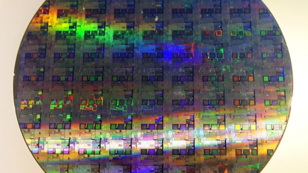
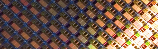
[Matt] has been working at Agilent / Keysight since 2007 as an ASIC designer. The work starts with code that is synthesized into logic gates. After that, [Matt] takes those gates and puts them into silicon. He’s worked with processes from 0.13um to 28nm. Turning code into silicon is still a dark art around here, and if you’ve ever wanted to know how all of this works, this is your chance to find out.

Here’s How To Take Part:

join-hack-chatOur Hack Chats are live community events on the Hackaday.io Hack Chat group messaging.

Log into Hackaday.io, visit that page, and look for the ‘Join this Project’ Button. Once you’re part of the project, the button will change to ‘Team Messaging’, which takes you directly to the Hack Chat.

You don’t have to wait until Friday; join whenever you want and you can see what the community is talking about.

Upcoming Hack Chats

We’ve got a lot on the table when it comes to our Hack Chats. On March 24th, we’re going to argue the merits of tube amplifiers in audio applications. In April, we have [Samy Kamkar], hacker extraordinaire, to talk reverse engineering.

Because I’ve never had the opportunity to do so, and because these Hack Chat announcement posts never get many comments anyway, I’m going to throw this one out there. What would it take to build out a silicon fabrication plant based on technology from 1972? I’m talking about a 10-micrometer process here, something that might be able to clone a 6502. Technology is on our side — a laser printer is cheaper than a few square feet of rubylith — and quartz tube heaters and wire bonding machines can be found on the surplus market. Is it possible to build a silicon fab in your garage without going broke? Leave your thoughts in the comments, and then bring them with you to the Hack Chat this Friday.