Get Down To The Die Level With This Internal Chip Repair

Usually, repairing a device entails replacing a defective IC with a new one. But if you’ve got young eyes and haven’t had caffeine in a week, you can also repair a defective chip package rather than replace it.

There’s no description of the incident that resulted in the pins of the QFP chip being ablated, but it looks like a physical insult like a tool dropped on the pins. [rasminoj]’s repair consisted of carefully grinding away the epoxy cap to expose the internal traces leading away from the die and soldering a flexible cable with the same pitch between the die and the PCB pads.

This isn’t just about [rasminoj]’s next-level soldering skills, although we’ll admit you’ve got to be pretty handy with a Hakko to get the results shown here. What we’re impressed with is the wherewithal to attempt a repair that requires digging into the chip casing in the first place. Most service techs would order a new board, or at best solder in a new chip. But given that the chip sports a Fanuc logo, our bet is that it’s a custom chip that would be unreasonably expensive to replace, if it’s even still in production. Where there’s a skill, there’s a way.

Need more die-level repairs? Check out this iPhone CPU repair, or this repair on a laser-decapped chip.

[via r/electronics]

CES2017: Complete Register Documentation For The C.H.I.P.

Last October, Next Thing Co., makers of the popular C.H.I.P. platform unleashed the C.H.I.P. Pro, a very capable Linux system on a tiny board. The goal of the C.H.I.P. Pro is to be the brains of a project or product, similar to the Gumstix boards from an ancient era long before the Raspberry Pi.

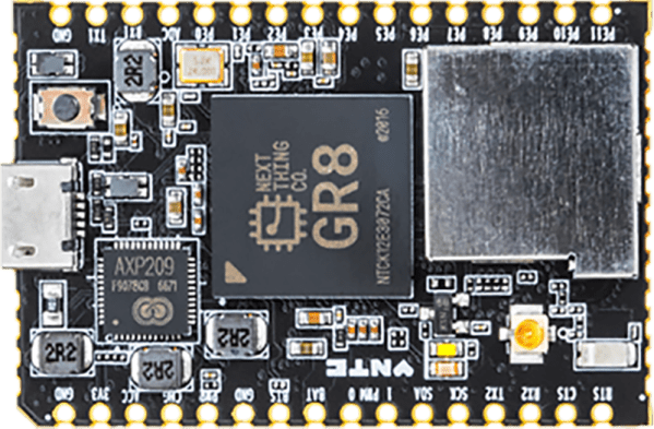
Introduced alongside the C.H.I.P. Pro was a fantastic little device. The GR8 module is a complete Linux system on a chip, with an ARM Cortex-A8 processor and 256 MB of RAM, all on a relatively small BGA chip. This is a drop-in part that gives any piece of hardware a Linux brain.

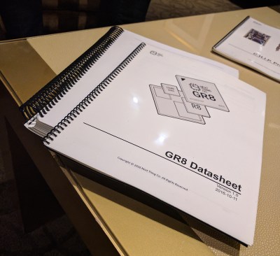
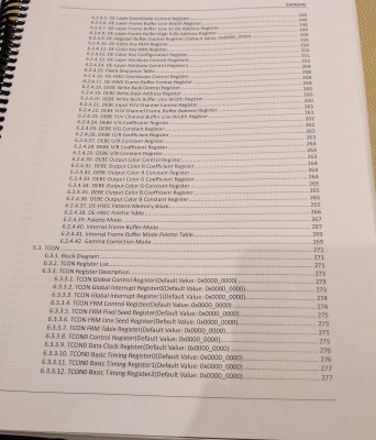
There was a datasheet at the time the C.H.I.P. Pro and GR8 module were released, but a datasheet can only go so far. What you really need to use a Linux system on a module is a massive tome filled with descriptions of registers and all the hardware nooks and crannies needed to get the part working. At CES this week, Next Thing Co. brought what everyone has been asking for: an NDA-free complete register documentation for the core they’re using on the GR8 module. This is 400 pages of spiral-bound goodness that will tell you how to do everything with this chip.

Using the C.H.I.P. for products

When the C.H.I.P. was first released, it was easy to write it off as a board glomming on to the popularity of the Raspberry Pi. However, Next Thing Co. didn’t start with the C.H.I.P. – they started with Otto, an animated gif camera built around the Raspberry Pi compute module. The Otto was successful, but the compute module is a little expensive, so Next Thing Co. turned their attention to building a modern, inexpensive version of the old Gumstix boards.

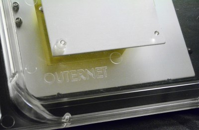
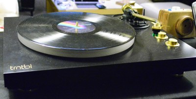
The C.H.I.P. Pro and GR8 is the culmination of this work, and already a few companies have used it in production. At the Next Thing Co. suite, they showed off a new version of the Outernet base station powered by the C.H.I.P. Pro, and the TRNTBL, a wireless, Bluetooth, Airplay, and Spotify-connected turntable.

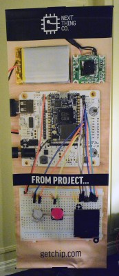
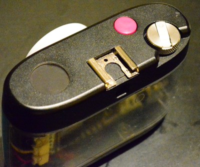
To illustrate how easy using the C.H.I.P. Pro in a product is, the guys at Next Thing Co. removed the Pi-powered guts of an Otto and replaced it with a C.H.I.P. Pro. There wasn’t much inside – just a battery, camera module, and a few bits and bobs. That’s great for anyone who wants to build a product that needs a relatively fast chip running Linux, and the stuff from Next Thing Co. makes it easy.

Ken Shirriff Takes Us Inside The IC, For Fun

[Ken Shirriff] has seen the insides of more integrated circuits than most people have seen bellybuttons. (This is an exaggeration.) But the point is, where we see a crazy jumble of circuitry, [Ken] sees a riddle to be solved, and he’s got a method that guides him through the madness.

In his talk at the 2016 Hackaday SuperConference, [Ken] stepped the audience through a number of famous chips, showing how he approaches them and how you could do the same if you wanted to, or needed to. Reading an IC from a photo is not for the faint of heart, but with a little perseverance, it can give you the keys to the kingdom. We’re stoked that [Ken] shared his methods with us, and gave us some deeper insight into a handful of classic silicon, from the Z80 processor to the 555 timer and LM7805 voltage regulator, and beyond.

Continue reading “Ken Shirriff Takes Us Inside The IC, For Fun”

NextThingCo Introduces C.H.I.P. Pro, GR8 System On Module

NextThingCo, makers of the very popular C.H.I.P. single board Linux computer, have released the latest iteration of their hardware. It’s the C.H.I.P. Pro, an SBC designed to be the embedded brains of your next great project, product, or Internet of Things thing.

The C.H.I.P. Pro features an Allwinner R8 ARMv7 Cortex-A8 running at 1 GHz, a MALI-400 GPU, and either 256 MB or 512 MB of NAND Flash. The Pro also features 802.11 b/g/n WiFi, Bluetooth 4.2, and is fully certified by the FCC. This board will be available in December at supposedly any quantity for $16.

The design of the C.H.I.P. Pro is a mix between a module designed to be installed in a product and a single board computer designed for a breadboard. It features castellated edges like hundreds of other modules, but the design means that assembly won’t be as simple as throwing down some paste and reflowing everything. The C.H.I.P. Pro features parts on two sides, making reflow questionable and either 0.1″ headers or a cutout on a PCB necessary. As a single board computer, this thing is small, powerful, and a worthy competitor to the Raspberry Pi Zero. A C.H.I.P. Pro development kit, consisting of two C.H.I.P. Pro units, a ‘debug’ board, and headers for breadboarding, is available for $49, with an estimated ship date in December.

A $16 Linux module with WiFi, Bluetooth, and no NDA is neat, but perhaps a more interesting announcement is that NextThingCo will also be selling the module that powers the C.H.I.P. Pro.

The GR8 module includes an Allwinner R8 ARMv7 Cortex-A8 running at 1 GHz, a MALI-400 GPU, and 256 MB of DDR3 SDRAM. Peripherals include TWI, two UARTS, SPI (SD cards support is hacked onto this), two PWM outputs, a single 6-bit ADC, I2S audio, S/PDIF, one USB 2.0 Host and one USB 2.0 OTG, and a parallel camera interface. This isn’t really a chip meant for video out, but it does support TV out and a parallel LCD interface. A limited datasheet for the GR8 is available on the NextThingCo GitHub.

Putting an entire Linux system on a single BGA module must draw comparisons to the recent release of the Octavo Systems OSD355X family, best known to the Hackaday audiences as the Beaglebone on a chip. Mechanically, the Octavo chip will be a bit easier to solder. Even though it has almost twice as many balls as the GR8, 400 on the Octavo and 252 on the GR8, the Octavo has a much wider pitch between the balls, making escape routing much easier.

Comparing peripherals between the OSD355X and GR8, it’s a bit of a wash, with the OSD coming out slightly ahead with Ethernet, more RAM and fancy TI PRUs. Concerning pricing, the GR8 wins hands down at $6 per chip in any quantity. That’s significantly less than the OSD355X.

The original C.H.I.P. has been exceptionally well received by the community NextThingCo is marketing to, despite the community’s distaste for Allwinner CPUs, cringeworthy PR, and questions concerning the true price of the C.H.I.P.. The C.H.I.P. Pro will surely see more than a few uses, but the GR8 is the real story here. A jellybean part that contains an entire Linux system has been the fevered dream of a madman for years now. The GR8 makes putting the power of open software into any project much easier, and we can’t wait to see the applications it allows.

A Peek Under The Hood Of The 741 Op-Amp

First introduced as an IC back in 1968, but with roots that go back to 1941, the 741 has been tweaked and optimized over the years and is arguably the canonical op-amp. [Ken Shirriff] decided to take a look inside everybody’s favorite op-amp, and ended up with some good-looking photomicrographs and a lot of background on the chip.

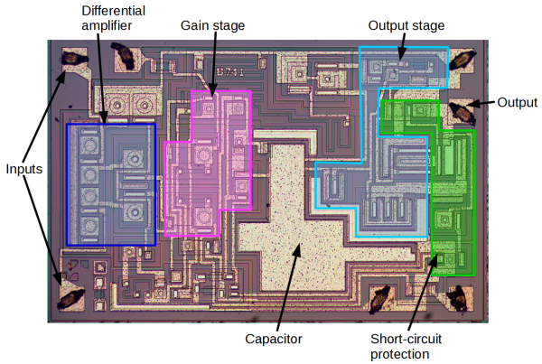
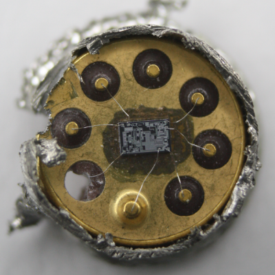
canRather than risk the boiling acid method commonly used to decap epoxy-potted ICs, [Ken] wisely chose a TO-99 can format to attack with a hacksaw. With the die laid bare for his microscope, he was able to locate all the major components and show how each is implemented in silicon. Particularly fascinating is the difference between the construction of NPN and PNP transistors, and the concept of “current mirrors” as constant current sources. And he even whipped up a handy interactive chip viewer – click on something in the die image and find out which component it is on the 741 schematic. Very nice.

We’ve seen lots of chip decappings before, including this reveal of TTL and CMOS logic chips. It’s nice to see the guts of the venerable 741 on display, though, and [Ken]’s tour is both a great primer for the newbie and a solid review for the older hands. Don’t miss the little slice of history he included at the end of the post.

The First 5nm Chip

For almost forty years, integrated circuits have become smaller and smaller. These chips started out with massive transistors in the early 1970s. They shrank to less than 1μm by 1990, and shrank yet again to less than 100nm by the turn of the last century. Now, Imec and Cadence are experimenting with 5nm technology – the smallest technology available for any mass-produced integrated circuit.

The history of microelectronic fabrication over the last decade is a story of failure. Something happened in 2005, and although chips could be designed at ever-smaller technologies, the transition to these smaller manufacturing processes didn’t go as smoothly as in the 70s, 80s, and 90s. Just a few years ago, Intel said 10nm chips would ship by 2015. These chips are nowhere to be found, and even 14nm technology is still catching up to the yields found in 22nm technology. In 2009, Nvidia said their flagship graphics card would be built with a 11nm process. The current Nvidia flagship desktop graphics card is built with 28nm technology. Moore’s law isn’t 18 months anymore.

While Imec and Cadence have completed the tapeout on a 5nm device, it’s just a test chip. Before starting manufacturing on a single process node, Intel and others will tapeout a simple test chip to verify their latest process. This 5nm tapeout will not become a manufactured chip, but it does mean we’ll see more talk about the 5nm process in the future.

How CMOS Works: Some Final Words About CMOS

Finishing up on the topic of CMOS bus logic I am going to show a couple of families with unique properties that may come in handy one day.

High Voltage Tolerant Family: AHC/AHCT

AHCT w/o high side diode
Note the missing diode to VDD

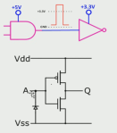
First up is a CMOS logic family  AHC/AHCT that has one of the protection diodes on the input removed.  This allows a 5V input voltage to be applied to a device powered by 3.3V so that I don’t have to add a gate just for the translation.  Any time I can translate and do it without any additional gate delays I am a happy engineer.

Of course the example above works in a single direction and bidirectional does start to get more complicated. Using a bidirectional buffer such as a 74AHCT245 will work for TTL translation when going from 3.3V back to 5V providing there is a direction control signal present.

Continue reading “How CMOS Works: Some Final Words About CMOS”