Oddball LCDs Reverse Engineered Thanks To Good Detective Work

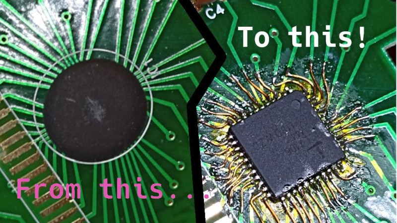
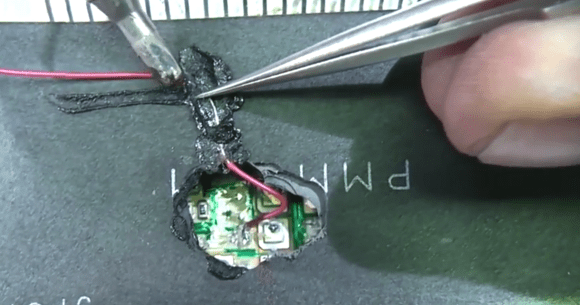
Is there anything more discouraging to the reverse engineer than to see a black blob of epoxy applied directly to a PCB? We think not, because that formless shape provides no clue as to what chip lies beneath, and that means a lot of detective work if you’re going to figure out how to use this thing.

[Sudhir Chandra]’s detective story starts with a bunch of oddball LCDs, slim 1×32 character units rather than the more familiar 2×16 displays. Each bore the dreaded black COB blob on the back, as well as a handful of SMD components and not much else. Googling revealed no useful documentation, and the manufacturer wasn’t interested in fielding calls from a hobbyist. Reasoning that most manufacturers wouldn’t spin up a custom chip for every display, [Sudhir] assumed there was an ST7066, a common LCD driver chip, underneath the blob, especially given the arrangement of external components. But a jumper set was bodged together under this assumption didn’t get the display going.

Next up were more destructive methods, to decap the COB and see what kind of numbers might be on the chip. Sandpaper worked at first, but [Sudhir] eventually turned to the “Chips a la [Antoine]” method of decapping, which uses heat and brute force to get at the goods. This got down to the chip, but [Sudhir]’s microscope wasn’t up to the task of reading the die markings.

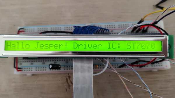
What eventually cracked the case was tracing out the voltages across the various external resistors and matching them up to other chips in the same family as the ST7066, plus the realization that the long, narrow epoxy blob probably covered a similarly shaped chip, which led to the culprit: an ST7070. This allowed [Sudhir] to build an adapter PCB for the displays, with plans for a custom Arduino library to talk to the displays.

This was a great piece of reverse engineering and a good detective story to boot. Hats off to [Sudhir] for sticking with it.

On the left, an image of a COB on the multimeter's PCB. On the right, a QFP IC soldered to the spot where a COB used to be, with pieces of magnet wire making connections from the QFP's pins to the PCB tracks.

Epoxy Blob Excised Out Of Broken Multimeter, Replaced With A QFP

The black blobs on cheap PCBs haunt those of us with a habit of taking things apart when they fail. There’s no part number to look up, no pinout to probe, and if magic smoke is released from the epoxy-buried silicon, the entire PCB is toast. That’s why it matters that [Throbscottle] shared his journey of repairing a vintage multimeter whose epoxy-covered single-chip-multimeter ICL7106 heart developed an internal reference fault. When a multimeter’s internal voltage reference goes, the meter naturally becomes useless. Cheaper multimeters, we bin, but this one arguably was worth reviving.

[Throbscottle] doesn’t just show what he accomplished, he also demonstrates exactly how he went through the process, in a way that we can learn to repeat it if ever needed. Instructions on removing the epoxy coating, isolating IC pins from shorting to newly uncovered tracks, matching pinouts between the COB (Chip On Board, the epoxy-covered silicon) and the QFP packages, carefully attaching wires to the board from the QFP’s legs, then checking the connections – he went out of his way to make the trick of this repair accessible to us. The Instructables UI doesn’t make it obvious, but there’s a large number of high-quality pictures for each step, too.

The multimeter measures once again and is back in [Throbscottle]’s arsenal. He’s got a prolific history of sharing his methods with hackers – as far back as 2011, we’ve covered his guide on reverse-engineering PCBs, a skillset that no doubt made this repair possible. This hack, in turn proves to us that, even when facing the void of an epoxy blob, we have a shot at repairing the thing. If you wonder why these black blobs plague all the cheap devices, here’s an intro.

We thank [electronoob] for sharing this with us!

The BGA chip in question flipped onto a piecce of breadboard, all its pins broken out with magnet wire.

Heroic Efforts Give Smallest ARM MCU A Breakout, Open Debugger

In today’s episode of Diminutive Device Technology Overview, [Sprite_TM] is at it again – this time conquering the HC32L110. A few weeks ago, we have highlighted the small ARM Cortex M0+ microcontroller, which is outstanding because of its exceptionally small size. We also pointed out a few hurdles, among them – hard-to-approach SDK and documentation, and difficulties making and assembling a PCB for such a small BGA. Today, we witness how [Sprite_TM] bulldozed through all of these hurdles for all of us, and added a few pictures to our collective “outrageous soldering” galleries while at it.

First, he figured out an example layout for this MCU that’s achievable for us even on a cheapest 2-layer board from JLCPCB, keeping distances within the generic tolerance standards by snubbing out a few pins. As a result, we only lose access to four GPIOs – those will have to be kept as inputs, so that nothing burns out. However, that’s the kind of tradeoff we are okay making if it helps us keep our PCB small and lightweight for projects where these factors matter. After receiving the resulting board, he also recorded a short tutorial on soldering such packages at home with a mere hot air gun and a few bare necessities like flux and tweezers – embedded below.

It doesn’t end there, however, as he decided to work around the GPIO fanout limitation in a non-intended way. Evidently, [Sprite_TM] decided to have some fun, taking a piece of regular 0.1″ spacing protoboard and deadbugging the chip with magnet wire, much to our amusement. The resulting contraption, pictured above, worked – and this is ever something you’d like to be able to achieve yourself in times of dire need, whether you make something work or simply to be entertained by making use of a cursed mounting technique, there’s an one-hour-long livestream recording of how this magnet wire contraption came to be. And, of course, that wasn’t the last thing to be shared.

Continue reading “Heroic Efforts Give Smallest ARM MCU A Breakout, Open Debugger”

The teeny tiny MCU mentioned in the article, merely a blimp on a giant devboard

New Part Day: Smallest ARM MCU Uproots Competition, Needs Research

We’ve been contacted by [Cedric], telling us about the smallest ARM MCU he’s ever seen – Huada HC32L110. For those of us into miniature products, this Cortex-M0+ package packs a punch (PDF datasheet), with low-power, high capabilities and rich peripherals packed into an 1.6mm x 1.4mm piece of solderable silicon.

This is matchstick head scale computing, with way more power than we previously could access at such a scale, waiting to be wrangled. Compared to an 8-bit ATTiny20 also available in WLCSP package, this is a notable increase in specs, with a way more powerful CPU, 16 times as much RAM and 8-16 times the flash! Not to mention that it’s $1 a piece in QTY1, which is about what an ATTiny20 goes for. Being a 0.35mm pitch 16-pin BGA, your typical board house might not be quite happy with you, but once you get a board fabbed and delivered from a fab worth their salt, a bit of stenciling and reflow will get you to a devboard in no time.

Drawbacks? No English datasheet or Arduino port, and the 67-page PDF we found doesn’t have some things like register mappings. LILYGO promised that they will start selling the devboards soon, but we’re sure it wouldn’t be hard for us to develop our own. From there, we’d hope for an ESP8266-like effect – missing information pieced together, translated and made accessible, bit by bit.

When it comes to soldering such small packages, we highly recommend reflow. However, if you decide to go the magnet wire route, we wouldn’t dare object – just make sure to send us pictures. After all, seems like miniature microcontrollers like ATTiny20 are attractive enough of a proposition that people will pick the craziest route possible just to play with one. They say, the madness of the brave is the wisdom of life.

We thank [Cedric] for sharing this with us!

COB LED Teardown

[Big Clive] picked up some chip-on-board (COB) LEDs meant for hydroponics that were very unusual and set out to examine them on video. Despite damaging the board almost right away, he managed to do some testing on these arrays and you can see the results in the video below. He also compares it to older LED modules.

The 144 LEDs produce a lot of light. In addition to powering the device up, he also looks at the construction of the LEDs under a magnification, comparing the older style that used tiny bond wires to make connections versus the new version soldered on the board directly.

Continue reading “COB LED Teardown”

The Mystery Behind The Globs Of Epoxy

When Sparkfun visited the factory that makes their multimeters and photographed a mysterious industrial process.

We all know that the little black globs on electronics has a semiconductor of some sort hiding beneath, but the process is one that’s not really explored much in the home shop.  The basic story being that, for various reasons , there is no cheaper way to get a chip on a board than to use the aptly named chip-on-board or COB process. Without the expense of encapsulating  the raw chunk of etched and plated silicon, the semiconductor retailer can sell the chip for pennies. It’s also a great way to accept delivery of custom silicon or place a grouping of chips closely together while maintaining a cheap, reliable, and low-profile package.

As SparkFun reveals, the story begins with a tray of silicon wafers. A person epoxies the wafer with some conductive glue to its place on the board. Surprisingly, alignment isn’t critical. The epoxy dries and then the circuit board is taken to a, “semi-automatic thermosonic wire bonding machine,” and slotted into a fixture at its base. The awesomely named machine needs the operator to find the center of the first two pads to be bonded with wire. Using this information it quickly bonds the pads on the silicon wafer to the  board — a process you’ll find satisfying in the clip below.

The final step is to place the familiar black blob of epoxy over the assembly and bake the board at the temperature the recipe in the datasheet demands. It’s a common manufacturing process that saves more money than coloring a multimeter anything other than yellow.

Continue reading “The Mystery Behind The Globs Of Epoxy”

Tricky Repair Of Power Driver For CNC Machine

tricky-power-driver-repair

Designing and building something from scratch is one thing. But repairing fried electronics is a much different type of dark art. This video from [Mike’s Electric Stuff] is from more than a year ago, but we didn’t think you’d mind since what he accomplishes in it is so impressive. He’s got a burnt out pick and place hybrid power module which isn’t going to fix itself.

The power module construction includes a part that has chip-on-board-style MOSFETs and the circuitry that goes with them enclosed in a black plastic housing. It’s kind of like a submodule was encapsulated using the same plastic as integrated circuits. After cracking it open it appears the bonding wire has burnt away. [Mike] connects a jumper wire to one of the board traces in order to use an external MOSFET. This is much easier said than done since the module substrate is ceramic designed to dissipate heat. We’re amused by his technique of melting the jumper into the plastic housing to protect it from the heat sink that goes over the package. In the end he gets his CNC running again. This may not be the best long-term fix but he just needed to continue running until a proper replacement part arrives.

Oh, one more thing: the Metcal vacuum desolderer he uses in the video… do want!

Continue reading “Tricky Repair Of Power Driver For CNC Machine”