Between manufacturing technologies like 3D-printing, CNC routers, lost-whatever metal casting, and laser and plasma cutters, professional quality parts are making their way into even the most modest of DIY projects. But stamping has largely eluded the home-gamer, what with the need for an enormous hydraulic press and massive machined dies. There’s more than one way to stamp parts, though, and the budget-conscious shop might want to check out this low-end hydroforming method for turning sheet metal into quality parts.
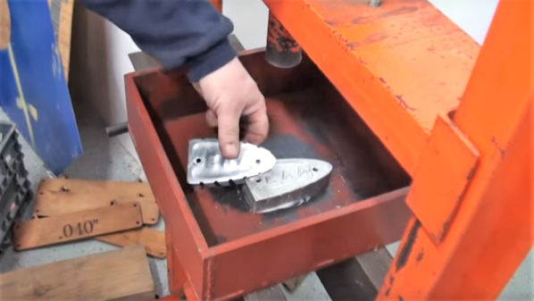
If hydroforming sounds familiar, it might be because we covered [Colin Furze]’s attempt, which used a cheap pressure washer to inflate sheet metal bubbles with high-pressure water. The video below shows a hydroformer that [Rainbow Aviation] uses (with considerably less screaming) to make stamped aluminum parts for home-brew aircraft. The kicker with this build is that there is no fluid — at least not until the 40,000-pound hydraulic press semi-liquifies the thick neoprene rubber pad placed over the sheet metal blank and die. The pressure squeezes the metal into and around the die, forming some pretty complex shapes in a single operation. We especially like the pro-tip of using Corian solid-surface countertop material offcuts to make the dies, since they’re available for a pittance from cabinet fabricators.
It’s always a treat to see hacks from the home-brew aviation world. They always seem to have plenty of tricks and tips to share, like this pressure-formed light cowling we saw a while back.
Continue reading “Low-Budget Hydroformer Puts The Squeeze On Sheet Metal Parts”


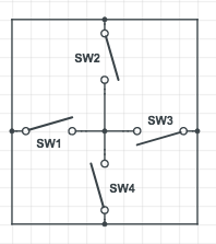 [Vejdemo-Johansson] figured a circle of 4 tilt sensors mounted on the one and twenty face would be enough to detect critical rolls. If any of the switches were tilted beyond 30 degrees, the switch would close. He mounted eight ball-tilt switches and glued in the LEDs. A hackerspace friend also helped him put together an astable multivibrator to generate the pulses for non-critical rolls.

 We have most recently seen [Ken] at work