As hackers approached the dramatic stone entrance of Portland’s Pacific Northwest College of Arts, a group of acolytes belonging to The Church of Robotron beckoned them over, inviting them to attempt to earn the title of Mutant Saviour. The church uses hazardous environments, religious indoctrination, a 1980s arcade game and some seriously funny low tech hacks to test your abilities to save humanity. This offbeat welcome was a pretty good way to set the tone for Teardown 2019: an annual Crowd Supply event for engineers and artists who love hardware. Teardown is halfway between a conference and a party, with plenty of weird adventures to be had over the course of the weekend. Praise the Mutant! Embrace Futility! Rejoice in Error!
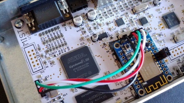
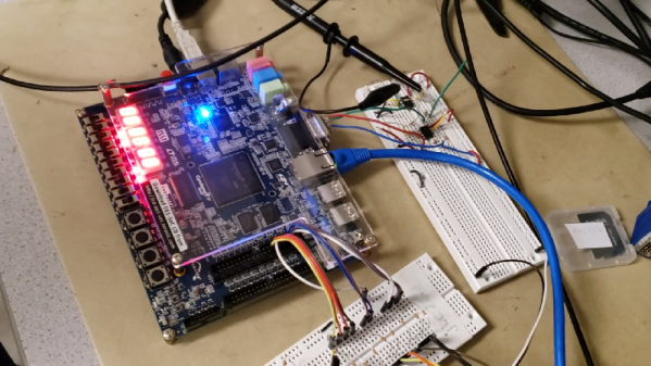
For those of us who failed to become the Mutant Saviour, there were plenty of consolation prizes. Kate Temkin and Mikaela Szekely’s talk on accessible USB tools was spectacular, and I loved following Sophi Kravitz’s journey as she made a remote-controlled blimp. Upstairs in the demo room, we had great fun playing with a pneumatic donut sprinkle pick and place machine from tinkrmind and Russell Senior’s hacked IBM daisywheel typewriter that prints ASCII art and runs a text-based Star Trek adventure game.
It wouldn’t be much of a hardware party if the end of the talks, demos and workshops meant the end of each day’s activities, but the Teardown team organised dinner and an afterparty in a different locations every night: Portland’s hackerspace ^H PDX, the swishy AutoDesk offices, and the vintage arcade game bar Ground Kontrol. There also was a raucous and hotly-contested scavenger hunt across the city, with codes to crack, locks to pick and bartenders to sweet talk into giving you the next clue (tip: tip).
Join me below for my favorite highlights of this three day (and night) festival.
Continue reading “Teardown 2019: A Festival Of Hacking, Art, And FPGAs”