Making Braille Signs Out Of PCBs

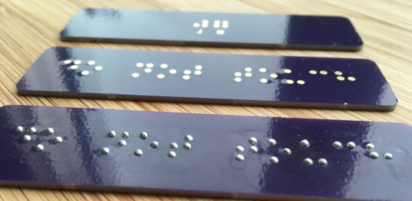
[jg] recently passed some damaged Braille signs and took on the challenge of repairing them. Informed by his recent work on PCB lapel pins, [jg] immediately thought of using circuit boards for this project. He’d noticed that round solder pads made for uniform hills of solder, and this reminded him of the bumps in Braille.

He began by reading up on the standards of the Braille Authority of North America, which stipulates a dot height of 0.6mm. He loaded up the PharmaBraille font system and laid it out the dots in photoshop, then and imported it into KiCad and laid out the boards. When the PCBs had arrived from OSH Park, [jg] soldering up the pads (lead free, but of course) to see if he could get the hills to 0.6mm. He’s experimenting with different methods of melting the solder to try to get more even results.

Braille interfaces crop up a surprising amount in hacker projects. This refreshable Braille display and keyboard and the Braigo LEGO Braille printer are prime examples.

[thanks, Drew!]

Heavily Hacked Printer For DIY PCBs

Sometimes we get tips that only leave us guessing as to how — and sometimes why — a project was built. Such is the case with this PCB printer; in this case, the build specifics are the only thing in question, because it puts out some pretty impressive PCBs.

All we have to go on is the video after the break, which despite an exhaustive minutes-long search appears to be the only documentation [Androkavo] did for this build. The captions tell us that the printer is built around the guts from an Epson Stylus Photo 1390 printer. There’s no evidence of that from the outside, as every bit of the printer has been built into a custom enclosure. The paper handling gear has been replaced by an A3-sized heated flatbed, adjustable in the Z-axis to accommodate varying board thicknesses. The bed runs on linear rails that appear custom-made. Under the hood, the ink cartridges have been replaced with outboard ink bottles in any color you want as long as it’s black. The video shows some test prints down to 0.1 mm traces with 0.1 mm pitch — those were a little dodgy, but at a 0.2 mm pitch, the finest traces came out great. The boards were etched in the usual way with great results; we wonder if the printer could be modified to print resist and silkscreens too.

[Androkavo] seems to have quite a few interesting projects in his YouTube channel, one of which — this wooden digital clock — we featured recently. We’d love to learn more about this printer build, though. Hopefully [Androkavo] will see this and comment below.

Continue reading “Heavily Hacked Printer For DIY PCBs”

Tinning Solution From The Hardware Store

Making your own printed circuit board at home often leads to a board which looks homemade. Exposed copper is one of the tell-tale signs. That may be your aesthetic and we won’t cramp your style, but exposed copper is harder to solder than tinned copper and it likes to oxidize over time. Tinning at home can bring you a step closer to having a full-featured board. In the video after the break, famed chemist [nurdrage] shows us how to make tinning solution at home in the video below the break.

There are only three ingredients to make the solution and you can probably find them all at a corner hardware store.

  • Hydrochloric acid. Also known as muriatic acid.
  • Solid lead-free solder with ≥ 95% tin
  • Silver polish containing thiourea

Everything to pull this off is in the first three minutes of the video. [nurdrage] goes on to explain the chemistry behind this reaction. It doesn’t require electricity or heat but heat will speed up the reactions. With this kind of simplicity, there’s no reason to make untinned circuit boards in your kitchen anymore. If aesthetics are very important, home tinning yourself allows you to mask off certain regions and have exposed copper and tin on the same board.

[nurdrage] is no stranger to Hackaday, he even has an article here about making your own PCB etchants and a hotplate to kick your PCB production into high gear.

Thanks for the tip, [drnbutyllithium].

Continue reading “Tinning Solution From The Hardware Store”

Chemotransfer For DIY PCBs

Making PCBs with the toner transfer method has been around since you could buy your traces at Radio Shack. There are a million techniques for removing copper from sheets of fiberglass, from milling to using resist pens, to the ubiquitous laser printer toner transfer. Here’s a technique we haven’t seen before. [Darko Volk] is calling this ‘chemotransfer’. It’s mostly a laser printer toner transfer process, but the toner is transferred from paper to copper with the help of a special mix of solvents.

This chemotransfer process is almost identical to the usual process of making a toner transfer PCB. First, the design is printed in reverse on dextrin-coated paper, the paper is placed down on polished copper, the entire assembly is sent through a laminator, and finally the board is etched with the chemical of your choice. The key difference here is a solvent applied to the copper just before the design is laid down. [Darko Volk] made a mixture of 25% “cleaning petrol” (benzene, naphtha, or gasoline, or some sort of light hydrocarbon, apparently), 5% linseed oil, and 70% isopropanol. This apparently aids in releasing the toner from the paper and sticking it down to the copper.

From there, the process is effectively a standard toner transfer process. [Darko Volk] is using a solution of sodium persulphate for the etch, and rigged a camera up to a CNC machine for the drilling.

This process can be expanded to two-layer boards very easily using a light table to align the layers of paper before placing them down on the copper. You can check out a video of the fabrication of a single side and double sided board below.

Thanks [Andrej] for the tip.

Continue reading “Chemotransfer For DIY PCBs”

Why Not Expose Your PCBs Through An LCD?

Most people who have dabbled in the world of electronic construction will be familiar in some form with the process of producing a printed circuit board by exposing a UV sensitive coating through a transparent mask, before moving on to etching. Older readers will have created their masks by hand with crêpe paper tape on acetate, while perhaps younger ones started by laser-printing from their CAD package.

How about a refinement of the process, one which does away with the acetate mask entirely? [Ionel Ciobanuc] may have the answer, in the form of an exposure through an LCD screen. The video below the break shows how it’s done, starting with a (probably a bit too lengthy) sequence on applying the photo-resist coating to the board, and then sitting LCD on top of UV lamp with the board positioned at the top of the pile.

It’s an interesting demonstration, and one that certainly removes a step in the process of PCB creation as it brings the pattern direct from computer to board without an intermediate. Whether or not it’s worth the expenditure on an LCD is up to you, after all a sheet of acetate is pretty cheap and if you already have a laser printer you’re good to go. We’re curious to know whether or not any plastic components in the LCD itself might be damaged by long-term exposure to intense UV light.

Continue reading “Why Not Expose Your PCBs Through An LCD?”

The Art Of Blinky Business Cards

Business cards are stuck somewhere between antiquity and convenience. On one hand, we have very convenient paperless solutions for contact swapping including Bluetooth, NFC, and just saying, “Hey, put your number into my phone, please.” On the other hand, holding something from another person is a more personal and memorable exchange. I would liken this to the difference between an eBook and a paperback. One is supremely convenient while the other is tactile. There’s a reason business cards have survived longer than the Rolodex.

Protocols and culture surrounding the exchange of cards are meant to make yourself memorable and a card which is easy to associate with you can work long after you’ve given your card away. This may seem moot if you are assigned cards when you start a new job, but personal business cards are invaluable for meeting people outside of work and you are the one to decide how wild or creative to make them.

Continue reading “The Art Of Blinky Business Cards”

Customizable PCB Business Card

[Corey Harding] designed his business card as a USB-connectable demonstration of his skill. If potential manager inserts the card in a USB drive, open a text editor, then touches the copper pad on the PCB, [Corey]’s contact info pops up in the text box.

In addition to working as a business card, the PCB also works as a Tiny 85 development board, with a prototyping area for adding sensors and other components, and with additional capabilities broken out: you can add an LED, and there’s also room for a 1K resistor, a reset button, or break out the USB’s 5V for other uses. There’s an AVR ISP breakout for reflashing the chip.

Coolly, [Corey] intended for the card to be an Open Source resource for other people to make their own cards, and he’s providing the Fritzing files for the PCB. Fritzing is a great program for beginning and experienced hardware hackers to lay out quick and dirty circuits, make wiring diagrams, and even export PCB designs for fabrication. You can download [Corey]’s files from his GitHub repository.

For another business card project check out this full color business card we published last month.