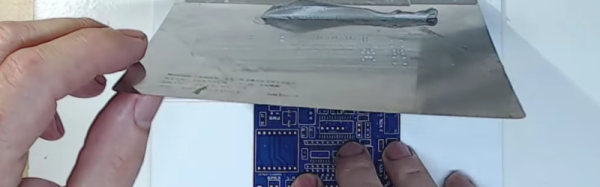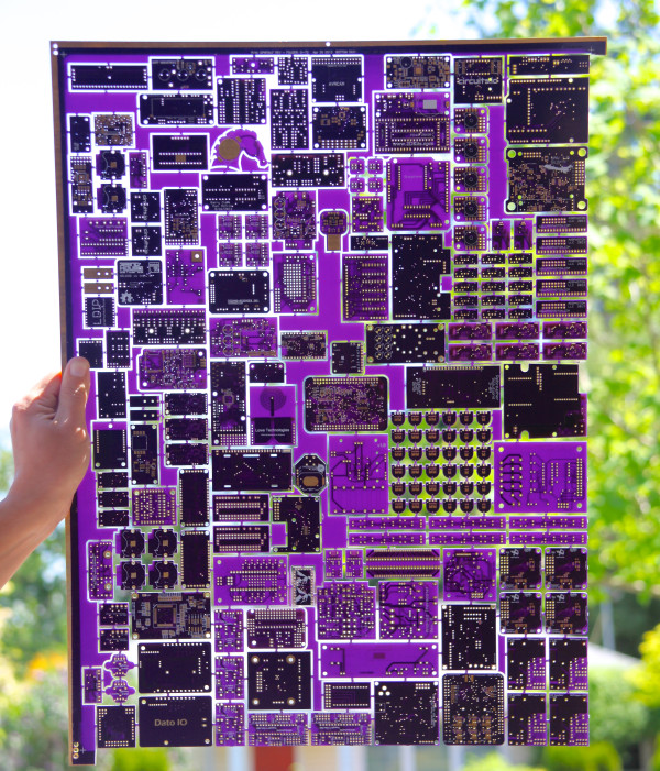
For those of us whose introduction to PCB making came decades ago and who share fond memories of permanent markers and crêpe paper sticky tape, the array of techniques available to PCB artists of today seem nothing short of magical. Toner transfer and peroxide etchant mixtures might seem run-of-the-mill to many readers, but even they are streets ahead of their predecessors from times past.
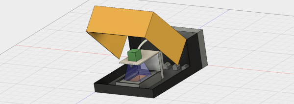
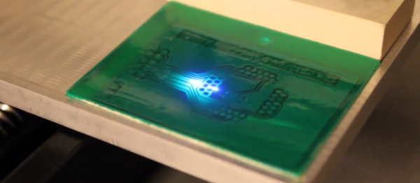
Photographic exposure of etch-resist coating has traditionally been performed with a UV lamp through a sheet of acetate film, but there is no reason why that should be the only way it can be performed. There have been plenty of projects using lasers or LEDs to draw a PCB design onto the coating as a raster, and a rather nice example from [Terje Io] using a Blu-Ray laser diode is the subject of the video below the break.
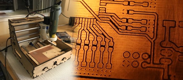
The diode is mounted on a gantry with a THK KR33 linear actuator that he tells us was unsuitable for his CNC mill due to backlash. This gives a claimed 1200 dpi resolution, over a 100 mm x 160 mm exposure area. Software is provided in a GitHub repository, taking a PNG image exported through a PDF printer. And since it’s got a UV laser, it can be used in a second pass to process UV-responsive soldermask film. ([Terje] cheats and uses a separate CNC mill to drill out the holes.) The result looks great.