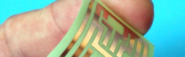
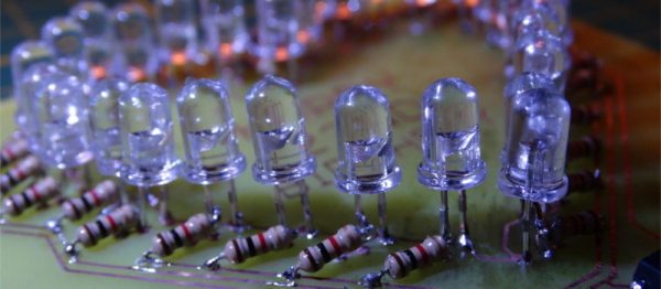
Creating A PCB In Everything: Introduction

engineering-drawingA few years ago, I wrote a few columns titled Making A Thing. These columns were a tutorial of sorts for several different 3D modeling programs. This column wasn’t meant to be a complete guide to modeling an object in OpenSCAD or SolidWorks, it was just step-by-step instructions on how to make one specific thing with one specific piece of software.

More than a few people in the Hackaday community found this column useful or at the very least an interesting pedagogical device. When starting out with any kind of productivity software, you don’t need to know how to do everything, you just need to know how to do the most common tasks.

Since the Making A Thing column was so popular, I felt it was time to revive this idea with another design task we often face. As you have already guessed, we’re going to be making printed circuit boards. Continuing the unique tutorial format created in the previous iteration of this column, Making a PCB will build one specific circuit in multiple EDA suites.

The Circuit

The entire concept of demonstrating how to build one thing in a specific software package necessitates a model thing. Before I even begin writing the first Making A PCB column, I need to design something that’s sufficiently complex but still relatively simple, and something that’s hopefully somewhat useful. Breakout boards are extremely simple, perhaps too much. In the course of these programs, I’ll need to demonstrate how to make a part in each specific software suite, so fewer pins are better.

Lacking any creativity of my own, I’ve settled on a very small ATtiny85 Arduino derivative from Tim a.k.a. [cpldcpu]. Tim’s Nanite 85 is an exceptionally small Arduino-compatible board based on the ATtiny85, complete with a USB port, LED, and a few pins of I/O. It’s simple but sufficiently complex to give an introduction to a PCB design suite.

I’m not going to outright copy Tim’s Nanite 85, though. It’s much clearer if parts aren’t stacked on top of each other, and I’d like to give myself a little breathing room on the layout. I’ve redesigned the circuit of the Nanite 85 to use mostly through-hole parts on a slightly larger board. I’m calling my version the Nanite Wesley, and if you get that reference, thumbs up for you.

ThingPCBSch
The schematic for the Nanite Wesley
naniteboard
The Nanite Wesley board. Copper pours not shown

Is this how a board should be laid out? No, absolutely not. I could probably do this as a single-layer board. This is a very inefficient layout, and I like rounded corners on my boards. It’s good enough, though, and it works. This is meant to be a tutorial on how to use a PCB design package, not a tutorial on how to design a PCB. Your criticisms in this regard are noted and ignored.

What These Tutorials Will Consist Of

You cannot use a PCB design package until you know how to make a part. Yes, Eagle has wonderful libraries for almost everything you can imagine, KiCad has plenty of parts on the Internet, and if you’re using a cloud-based PCB software, almost everything will be provided for you. If you make a PCB, eventually you’ll have to make your own part, though, and each tutorial will begin with making a DIP-8 ATtiny85. Everything else on this board is a jellybean part. Either way, the process of making a part and package for a Zener is the same as making one for a microcontroller.

The next part of the tutorial will consist of schematic capture. This means placing the parts in the schematic, drawing wires between the pins and pads, and naming them. From there, it’s time to actually make a board, and this means dropping the parts down, putting traces between all the pins, doing the board outline, pouring copper, and mechanical considerations.

With the schematic and board designed, it will be time to send it off to a fab house. For Eagle and KiCad, this is easy; OSHpark accepts Eagle .brd and KiCad .pcb files, but this is cheating. We’re going to use CAM to generate real Gerber files. If you make enough PCBs, you’ll have to learn it eventually.

Caveats and Poor Design

There are a lot of things that go into making a ‘proper’ PCB, including isolation, direct traces to decoupling capacitors, making sure pixies don’t go around sharp corners and a thousand other items that won’t be discussed in these tutorials. There’s a reason I won’t be discussing this. This is a guide on how to use a PCB design tool, not how to design a PCB.

What else should I do?

As you can probably guess from the schematic above, the first PCB software I’m going to cover is Eagle. KiCad is on the list, as is Fritzing, Altium CircuitMaker, and OrCAD. In the interests of putting PCB design in a historical context, I have a copy of AutoTRAX and an old DOS machine. I’ll also be covering a few of the cloud-only design tools such as Upverter.

That’s enough software suites to get started, but as with the Making A Thing series, I’m going to be looking for suggestions from the peanut gallery. I can’t change the circuit I’m making, as that’s the entire point of this series, but I am looking for suggestions on other tools to cover. What else can I do? Want me to grab a piece of copper clad board, sticker overlays, and some photostatic film? I can do that. Are you at a web-based EDA startup, and want some free advertising? Leave a note in the comments.

Thanks to our efforts to slowly improve the backend of Hackaday, you’ll be able to access all the Making A PCB In Everything posts from the series list below.

Vacuum Exposure Unit Gives Better PCB Etching Results

PCB etching seems to be a subject that sharply divides our community into those who are experts in it and etch themselves every PCB they use, and those who have significant quantities of ferric chloride stained clothing in their past and for whom the advent of cheap commercial PCB manufacture and CNC milled PCB prototyping have been the best thing since sliced bread.

Your likely success when etching your own boards is most dependent on the quality of your preparation and your equipment. If you began your PCB career with etch-resist transfers and a permanent marker with a Tupperware tub of etchant, then later progressed to laser toner or photographic masking and a bubble etcher, you’ll understand this.

[Jana Marie Hemsing] has drawn our attention to this very nicely built PCB etching suite (Translation, German original) at the Warpzone hackerspace (Translation, German original) in Münster, Germany. The foil pattern is printed on transparency and exposed to UV light over a photoresist coated board with a vacuum pump arrangement to ensure as good a contact as possible to the board for the sharpest result. They have two exposers, one for single sided and the other for double-sided boards, both are very well-built from what looks like plywood.

The attention to detail continues with a home-made magnetic stirrer and heated bubble etching tank Their etchant of choice is sodium persulphate, so there are none of those brown ferric chloride stains.

PCB etching is nothing new, indeed we have covered the subject extensively over the years. But we think you’ll agree, if you’re going to etch your own PCBs you should have as good a set-up as you can, and Warpzone’s PCB suite is rather well put together. Those of us in spaces with lesser facilities should be getting ideas from it.

Take Your PCBs From Good To Great: Toner Transfer

dscf8697
One-offs that I never would have gotten professionally made, but that were infinitely handy during development

A lot of us make circuit boards at home. I find it a useful skill to have in my bag of tricks for intermediate steps along the way to a finished project, even if the finished version is going to be sent out to a PCB fab. When I need a breakout board that meshes with other development tools, for instance, there’s nothing like being able to whip something up that plugs right in. Doing it quickly, and getting on with the rest of the project instead of placing an order and waiting for delivery, helps keep me in the flow.

Toner transfer is by far the fastest way to make a circuit board at home — simply print the circuit out on a laser printer, iron it onto the copper, and etch. When it works, it’s awesome. When it doesn’t, it can be a hair-pulling exercise in figuring out which of myriad factors are misaligned.

For a long time now, I’ve been using a method that’s very reliable and repeatable. Recently, I’ve been tweaking a bit on the performance of the system, and I thought I’d share what I’ve got. At the moment, I’m able to very reliably produce boards with 6 mil (0.15 mm) traces and 8 mil (0.20 mm) spacing. With a little care in post-production, 4 mil / 6 mil is entirely plausible.

Continue reading “Take Your PCBs From Good To Great: Toner Transfer”

The Evolution Of A DIY Circuit Board Plotter

In this three part video series we watch [Dirk Herrendoerfer] go from scraps to a nice 3D printed assembly as he iterates through the design of a pen plotter for making circuit boards.

[dana] mentioned [Dirk]’s work in the comments of this post which describes a different process. Many permanent markers stick to copper well enough to last through the chemical etching process. While hand drawing definitely produces some cool, organic-looking boards, for sharp lines and SMDs it gets a bit harder; to the point where it becomes advisable to just let a robot do it.

Of course, [Dirk] was aware of this fact of life. He just didn’t have a robot on hand. He did have some electronic detritus, fishing line, an Arduino, scrap wood, brass tubes, and determination.  The first version‘s frame consisted of wooden blocks set on their ends with holes drilled to accept brass rods. The carriage was protoboard and hot glue. Slightly larger brass tubing served as bushings and guide. As primitive as it was the plotter performed admirably, albeit slowly.

The second version was a mechanical improvement over the first, but largely the same. The software got a nice improvement. It worked better and had some speed to it.

The latest version has some fancy software upgrades; such as acceleration. The frame has gone from random bits of shop trash to a nicely refined 3D printed assembly. Even the steppers have been changed to the popular 28BYJ-48 series. All the files, software and hardware, are available on GitHub. The three videos are viewable after the break. It’s a great example of what a good hacker can put together for practically no money.

Continue reading “The Evolution Of A DIY Circuit Board Plotter”

Etching A PCB In Ten Minutes.

Most circuit boards any maker could need for their projects can be acquired online at modest cost, but what if you need something specific? [Giorgos Lazaridis] of pcbheaven.com has designed his own etching bath complete with a heater and agitator to sped up the process of creating your own custom circuit boards.

[Lazaridis] started by building a circuit to control — in a display of resourcefulness — a fish tank heater he would later modify. The circuit uses a PIC 16F526 microcontroller and two thermristors to keep the temperature of the etching bath between 38 and 41 degrees Celsius. The fish tank heater was gingerly pried from its glass housing, and its bimetallic strip thermostat removed and replaced with a wire to prevent it shutting off at its default 32 degrees. All of it is mounted on a small portable stand and once heated up, can etch a board in less than 10 minutes.

Continue reading “Etching A PCB In Ten Minutes.”

Escalating To CNC Through Proxxon’s Tool Line

Proxxon is a mostly German maker of above average micro tools. They do sell a tiny milling machine in various flavors, from manual to full CNC. [Goran Mahovlić] did not buy that. He did, however, combine their rotary tool accessory catalog into a CNC mill.

Owning tools is dangerous. Once you start, there’s really no way to stop. This is clearly seen with Goran’s CNC machine. At first happiness for him was a small high speed rotary tool. He used it to drill holes in PCBs.

In a predictable turn of events, he discovered drilling tiny holes in PCBs by hand is tedious and ultimately boring. So he purchased the drill press accessory for his rotary tool.

Life was good for a while. He had all the tools he needed, but… wouldn’t it be better if he could position the holes more quickly. He presumably leafed through a now battered and earmarked Proxxon catalog and ordered the XY table.

A realization struck. Pulling a lever and turning knobs! Why! This is work for a robot, not a man! So he pestered his colleague for help and they soon had the contraption under CNC control.

We’d like to say that was the end of it, and that [Goran] was finally happy, but he recently converted his frankenmill to a 3D printer. We’ve seen this before. It won’t be long before he’s cleaning out his garage to begin the restoration and ultimate CNC conversion of an old knee mill. Videos after the break.

Continue reading “Escalating To CNC Through Proxxon’s Tool Line”

Taking The Converted PC PSU Bench Supply A Step Further

A quality bench power supply is essential for electronics work. Nobody wants to go through the trouble of digging through their electronics bin just to find a wall wart with the right output. And, even if you were so inclined, it would be folly to assume that its output would actually be clean.

You could, of course, purchase a purpose-built bench power supply. But, this is Hackaday, and I’m sure many of you would rather build one yourself from an inexpensive PC power supply. Normally, you’d do this by separating out the different voltage lines into useful groups, such as 12V, 5V, and 3.3V. [Supercap2f] wanted to take this a step further, both to get a more useful unit and to practice his PCB-making.

His design uses a custom circuit design to fuse the circuits, and to provide some basic logic. Using the LCD display, you can see which lines are powered on. There is even a simple 3D printed cover to keep everything neat and tidy. [Supercap2f] has posted all of the design files, so you can build one of these yourself. We’ve seen similar builds in the past, but this is another nice one that anyone with the ability to etch PCBs can build.