If you’ve ever tried to build a printed circuit board from home, you know how much of a pain it can be. There are buckets of acid to lug around, lots of waiting and frustration, and often times the quality of the circuits that can be made traditionally with a home setup isn’t that great in the end. Luckily, [Rich] has come up with a way that eliminates multiple prints and the acid needed for etching.
His process involves using a laser printer (as opposed to an inkjet printer, as is tradition) to get a layer of silver adhesive to stick to a piece of paper. The silver adheres to the toner like glitter sticks to Elmer’s glue, and allows a single pass of a laser printer to make a reliable circuit. From there, the paper can be fastened to something more solid, and components can be reflow soldered to it.
[Rich] does post several warnings about this method though. The silver is likely not healthy, so avoid contact with it, and when it’s applied to the toner an indeterminate brown smoke is released, which is also likely not healthy. Warnings aside, though, this is a great method for making home-made PCBs, especially if you don’t want tubs of acid lying around the house, however useful.
What’s your favorite value of resistor? 1K? 10K? They’re all fine, but when you need nearly no resistance at all, nothing beats the good old zero-ohm resistor.
Wait a minute! Resistors are supposed to resist current. What the heck does a zero-ohm resistor do? Well, the short story (tee-hee!) is that it’s like a jumper for single-sided surface-mount boards. In the bad old days, companies used to save money by running single-sided boards, and you could buy wire jumpers to help make the layout that much easier.
Fast forward to the modern era, where there’s not a through-hole component to be seen. What’s the resistance (ideally) of a wire? Zero ohms. And thus the zero-ohm resistor was born. We have a whole spool of them in our closet in 1206, the largest SMD size that we use, in order to be able to sneak two or three tracks underneath, even on a home-etched board. They’re great.
Anyway, what set us off rhapsodizing about the lowest value resistor was this article on the peculiarities of the zero ohm resistor. Of course, nothing has zero resistance, and the article walks you through some of their real-world properties. Enjoy!
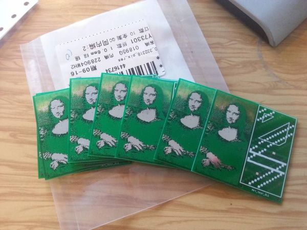
Many of us have held a circuit board up to a strong light to get a sense for how many layers of circuitry it might contain. [alongruss] did this as well, but, unlike us, he saw art.
We’ve covered some art PCBs before. These, for the most part, were about embellishing the traces in some way. They also resulted in working circuits. [alongruss]’s work focuses more on the way light passes through the FR4: the way the silkscreen adds an interesting dimension to the painting, and how the tin coating reflects light.
To prove out and play with his algorithm he started with GIMP. He ran the Mona Lisa through a set of filters until he had layers of black and white images that could be applied to the layers of the circuit board. He ordered a set of boards from Seeed Studio and waited.
They came back a success! So he codified his method into Processing code. If you want to play with it, take a look at his GitHub.
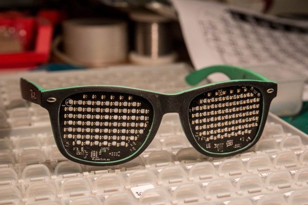
[Gal Pavlin] admits to enjoying the occasional dance music show. For those who have never been to one, LED one-upmanship at these shows is a real and terrible thing, so much so that an entire market exists around it. To that end, [Gal] built a pretty spiffy set of LED glasses.
It took quite a bit of work to arrive at the final design. All the circuitry and LEDs fit entirely within the envelope of the lenses on a pair of sunglass frames of dubious parentage. The batteries squeeze in between the user’s head and temples.
On top of the clever packaging is an equally impressive set of features. Each lens is a matrix of 69 LEDs. They have an accelerometer, a microphone, and a light sensor. There’s even a vibrating alert motor, which we feel is just showing off. Best of all, you can actually see through the glasses, thanks to clever layout and very tiny LEDs.
The device requires a tag connect or soldering on a pigtail to program. If you’d like to build one yourself all the files are available on [Gavin]’s site. There’s a video of it in operation after the break.
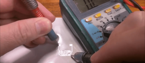
We’ve done a lot of PCBs with the toner transfer method over the years. The idea is simple: print a pattern using toner (which is just ground up black plastic) and then use an iron or other heat and pressure device to transfer the toner to a copper-clad board. It works and it works well. But getting just the right combination of heat, pressure, release paper, and toner is sometimes tricky.
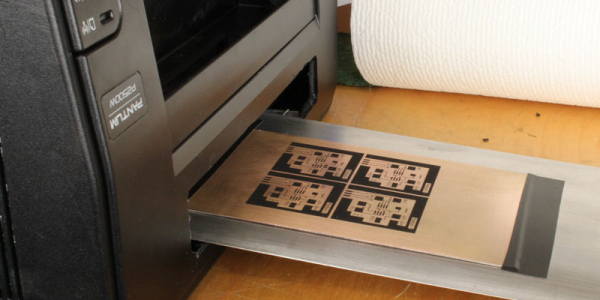
Some people hack their printers to turn off the fuser wire (to make the toner not stick to the paper) or to run a PCB directly through it. If you have a big expensive laser printer, though, you might not want to chop it up just to run PCBs. Have you looked at laser printer prices lately? We aren’t sure if it is cheap units flooding the market, or the overwhelming popularity of color printers, but you can pick up a Pantum P2500 for about $25 or $30–and probably get WiFi printing at that price. [Mlermen] picked one of these up and shows you how to convert it to a PCB printer.
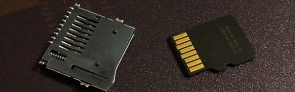
You do not know how to make a PCB unless you can make your own parts. [Jan] knows this, but like everyone else he checked out the usual online sources for a footprint for an SD card socket before making his own. It turns out, this SD card socket bought from an online marketplace was completely undocumented. Not only was an Eagle or KiCad footprint unavailable, but CAD files showing the dimensions of the part were non-existent. A solution had to be devised.
Instead of taking calipers and finely measuring all the pads on this SD card socket – a process that would surely fail – [Jan] decided to use a flatbed scanner to trace out the part. The part was placed on the glass and scanned at 300 dpi with a convenient reference object (a public transport card) in the same picture. This picture was imported into a CAD package, scaled to the correct ratio, and exported as a DXF. Since KiCad readily accepts importing DXFs, the CAD file was easily accessed, traced over, and a new part created.
From start to finish, making the footprint for this no-name, off-brand SD card socket took fifteen minutes. That’s nothing compared to the time it would take to manually measure each of the pads, draw a footprint, and print out the footprint at 1:1 scale to see if it matched up several times. It’s awesome work, and a great reminder that the best tools are usually right in front of you.
A few years ago, I wrote a few columns titled Making A Thing. These columns were a tutorial of sorts for several different 3D modeling programs. This column wasn’t meant to be a complete guide to modeling an object in OpenSCAD or SolidWorks, it was just step-by-step instructions on how to make one specific thing with one specific piece of software.
More than a few people in the Hackaday community found this column useful or at the very least an interesting pedagogical device. When starting out with any kind of productivity software, you don’t need to know how to do everything, you just need to know how to do the most common tasks.
Since the Making A Thing column was so popular, I felt it was time to revive this idea with another design task we often face. As you have already guessed, we’re going to be making printed circuit boards. Continuing the unique tutorial format created in the previous iteration of this column, Making a PCB will build one specific circuit in multiple EDA suites.
The Circuit
The entire concept of demonstrating how to build one thing in a specific software package necessitates a model thing. Before I even begin writing the first Making A PCB column, I need to design something that’s sufficiently complex but still relatively simple, and something that’s hopefully somewhat useful. Breakout boards are extremely simple, perhaps too much. In the course of these programs, I’ll need to demonstrate how to make a part in each specific software suite, so fewer pins are better.
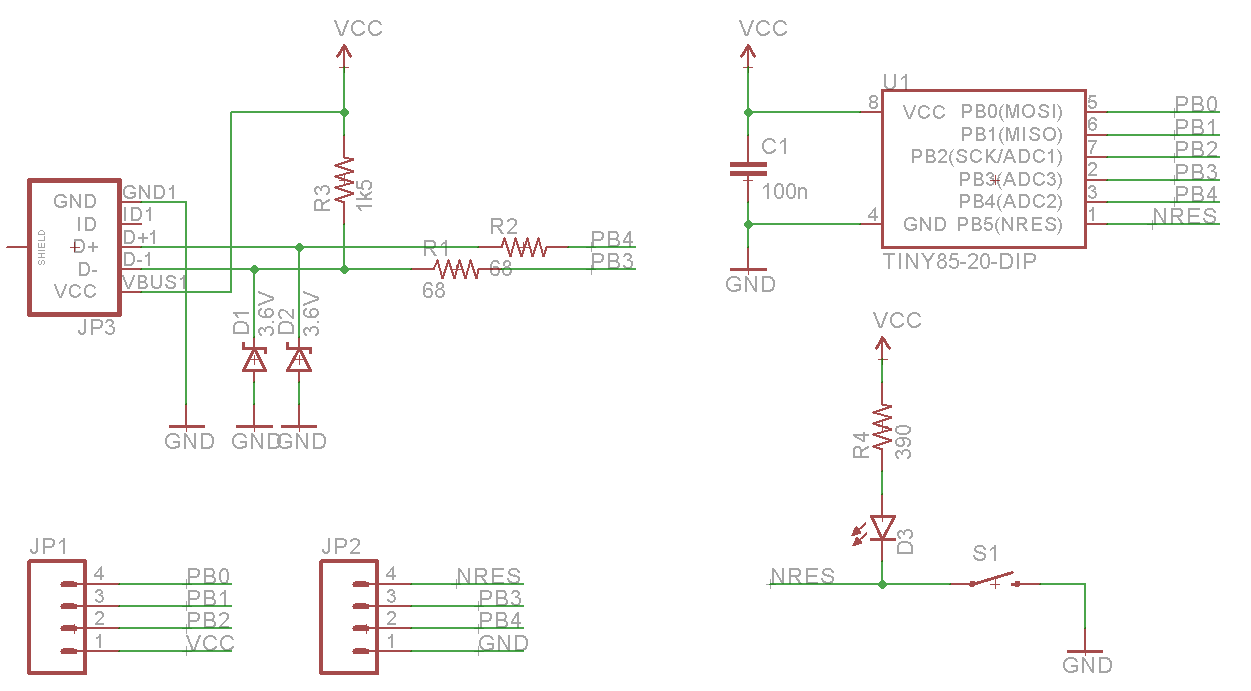
Lacking any creativity of my own, I’ve settled on a very small ATtiny85 Arduino derivative from Tim a.k.a. [cpldcpu]. Tim’s Nanite 85 is an exceptionally small Arduino-compatible board based on the ATtiny85, complete with a USB port, LED, and a few pins of I/O. It’s simple but sufficiently complex to give an introduction to a PCB design suite.
I’m not going to outright copy Tim’s Nanite 85, though. It’s much clearer if parts aren’t stacked on top of each other, and I’d like to give myself a little breathing room on the layout. I’ve redesigned the circuit of the Nanite 85 to use mostly through-hole parts on a slightly larger board. I’m calling my version the Nanite Wesley, and if you get that reference, thumbs up for you.
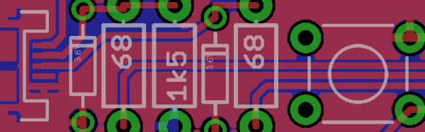
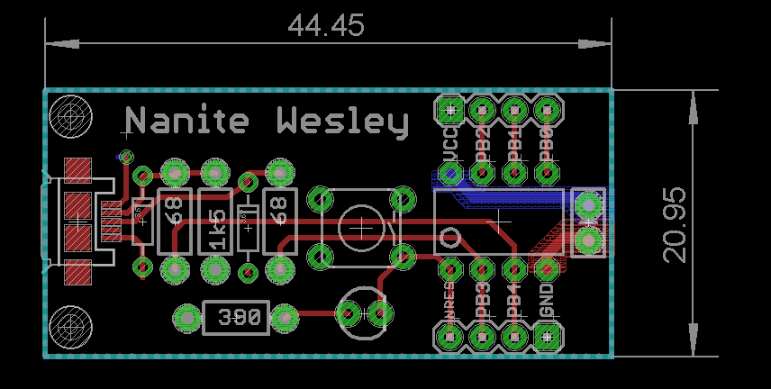
The schematic for the Nanite WesleyThe Nanite Wesley board. Copper pours not shown
Is this how a board should be laid out? No, absolutely not. I could probably do this as a single-layer board. This is a very inefficient layout, and I like rounded corners on my boards. It’s good enough, though, and it works. This is meant to be a tutorial on how to use a PCB design package, not a tutorial on how to design a PCB. Your criticisms in this regard are noted and ignored.
What These Tutorials Will Consist Of
You cannot use a PCB design package until you know how to make a part. Yes, Eagle has wonderful libraries for almost everything you can imagine, KiCad has plenty of parts on the Internet, and if you’re using a cloud-based PCB software, almost everything will be provided for you. If you make a PCB, eventually you’ll have to make your own part, though, and each tutorial will begin with making a DIP-8 ATtiny85. Everything else on this board is a jellybean part. Either way, the process of making a part and package for a Zener is the same as making one for a microcontroller.
The next part of the tutorial will consist of schematic capture. This means placing the parts in the schematic, drawing wires between the pins and pads, and naming them. From there, it’s time to actually make a board, and this means dropping the parts down, putting traces between all the pins, doing the board outline, pouring copper, and mechanical considerations.
With the schematic and board designed, it will be time to send it off to a fab house. For Eagle and KiCad, this is easy; OSHpark accepts Eagle .brd and KiCad .pcb files, but this is cheating. We’re going to use CAM to generate real Gerber files. If you make enough PCBs, you’ll have to learn it eventually.
Caveats and Poor Design
There are a lot of things that go into making a ‘proper’ PCB, including isolation, direct traces to decoupling capacitors, making sure pixies don’t go around sharp corners and a thousand other items that won’t be discussed in these tutorials. There’s a reason I won’t be discussing this. This is a guide on how to use a PCB design tool, not how to design a PCB.
What else should I do?
As you can probably guess from the schematic above, the first PCB software I’m going to cover is Eagle. KiCad is on the list, as is Fritzing, Altium CircuitMaker, and OrCAD. In the interests of putting PCB design in a historical context, I have a copy of AutoTRAX and an old DOS machine. I’ll also be covering a few of the cloud-only design tools such as Upverter.
That’s enough software suites to get started, but as with the Making A Thing series, I’m going to be looking for suggestions from the peanut gallery. I can’t change the circuit I’m making, as that’s the entire point of this series, but I am looking for suggestions on other tools to cover. What else can I do? Want me to grab a piece of copper clad board, sticker overlays, and some photostatic film? I can do that. Are you at a web-based EDA startup, and want some free advertising? Leave a note in the comments.
Thanks to our efforts to slowly improve the backend of Hackaday, you’ll be able to access all the Making A PCB In Everything posts from the series list below.