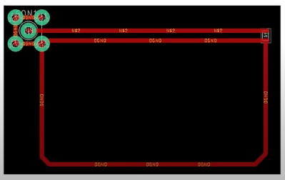
A Simple Guide To RF PCB Design

[Hans Rosenberg] knows a thing or two about RF PCB design and has provided a three-part four-part video demonstration of some solid rules of thumb. We will cover the first part here and leave the other two for the more interested readers!

The design process begins with a schematic diagram, assuming ideal conductors. Advanced software tools can extract the resistive, inductive, and capacitive elements of the physical wiring to create a parasitic model that can be compared to the desired schematic. The RF designer’s task is to optimize the layout to minimize differences and achieve the best performance to meet the design goals. However, what do you do when you don’t have access to such software?

[Hans] explains that at low frequencies, return current flows through all paths, with the lowest resistance path taking most of the current. At higher frequencies, the lowest inductance path carries all the current. In real designs, a ground plane is used instead of an explicit return trace for the lowest possible impedance.

You really wouldn’t design an RF circuit like this.

[Hans] shows the effect of interrupting the signal return path on a physical test PCB. The result is pretty bad, with the current forced to detour around the hole in the ground plane. A nanoVNA shows a -20 dB drop at 4 GHz, where the ground plane has effectively become an antenna. Energy will be radiated out, causing signal loss, but worse, it will create an EMC hazard with an unintended transmission.

Additionally, this creates an EMC susceptibility, making the situation worse. Placing a solder blob to bridge the gap directly under the signal trace is all that’s required to make it a continuous straight path again, and the performance is restored.

Floating planes are also an issue in RF designs, causing signal resonance and losses. One solution is to pull back the planes near the signal or stitch them to the ground plane with vias placed closely on either side of the signal trace. However, such stitching may slightly affect transmission line impedance and require tweaking the design a little. The next two parts of the series expand on this, hammering home the importance of good ground plane design. These are definitely worth a watch!

PCB design is as much art as science, and we’ve discussed this subject a lot. Here’s our simple guide to rocking RF PCB designs. There’s also a lot of devil in that detail, for example when understanding edge-launch SMA connectors.

Continue reading “A Simple Guide To RF PCB Design”

Coax Stub Filters Demystified

Unless you hold a First Degree RF Wizard rating, chances are good that coax stubs seem a bit baffling to you. They look for all the world like short circuits or open circuits, and yet work their magic and act to match feedline impedances or even as bandpass filters. Pretty interesting behavior from a little piece of coaxial cable.

If you’ve ever wondered how stub filters do their thing, [Fesz] has you covered. His latest video concentrates on practical filters made from quarter-wavelength and half-wavelength stubs. Starting with LTspice simulations, he walks through the different behaviors of open-circuit and short-circuit stubs, as well as what happens when multiple stubs are added to the same feedline. He also covers a nifty online calculator that makes it easy to come up with stub lengths based on things like the velocity factor and characteristic impedance of the coax.

It’s never just about simulations with [Fesz], though, so he presents a real-world stub filter for FM broadcast signals on the 2-meter amateur radio band. The final design required multiple stubs to get 30 dB of attenuation from 88 MHz to 108 MHz, and the filter seemed fairly sensitive to the physical position of the stubs relative to each other. Also, the filter needed a little LC matching circuit to move the passband frequency to the center of the 2-meter band. All the details are in the video below.

It’s pretty cool to see what can be accomplished with just a couple of offcuts of coax. Plus, getting some of the theory behind those funny little features on PCBs that handle microwave frequencies is a nice bonus. This microwave frequency doubler is a nice example of what stubs can do.

Continue reading “Coax Stub Filters Demystified”

Cavity Filters, The Black Art You Have A Chance Of Pursuing

A tuned circuit formed by a capacitor and an inductor is a familiar enough circuit, and it’s understood that it will resonate at a particular frequency. As that frequency increases, so the size of the capacitor and inductor decrease, and there comes a point at which they can become the characteristic capacitance and inductance of a transmission line. These tuned circuits can be placed in an enclosure, at which they can be designed for an extremely high Q factor, a measure of quality, and thus a very narrow resonant point. They are frequently used as filters for that reason, and [Fesz] is here with a video explaining some of their operation and configurations.

Some of the mathematics behind RF design can be enough to faze any engineer, but he manages to steer a path away from that rabbit hole and explain cavity filters in a way that’s very accessible. We learn how to look at tuned circuits as transmission lines, and the properties of the various different coupling methods. Above all it reveals that making tuned cavities is within reach.

They’re a little rare these days, but there was a time when almost every TV set contained a set of these cavities which were ready-made for experimentation.

Continue reading “Cavity Filters, The Black Art You Have A Chance Of Pursuing”

This Open Source Active Probe Won’t Break The Bank

If you’re like us, the oscilloscope on your bench is nothing special. The lower end of the market is filled with cheap but capable scopes that get the job done, as long as the job doesn’t get too far up the spectrum. That’s where fancier scopes with active probes might be required, and such things are budget-busters for mere mortals.

Then again, something like this open source 2 GHz active probe might be able to change the dynamics a bit. It comes to us from [James Wilson], who began tinkering with the design back in 2022. That’s when he learned about the chip at the center of this build: the BUF802. It’s a wide-bandwidth, high-input-impedance JFET buffer that seemed perfect for the job, and designed a high-impedance, low-capacitance probe covering DC to 2 GHz probe with 10:1 attenuation around it.

[James]’ blog post on the design and build reads like a lesson in high-frequency design. The specifics are a little above our pay grade, but the overall design uses both the BUF802 and an OPA140 precision op-amp. The low-offset op-amp buffers DC and lower frequencies, leaving higher frequencies to the BUF802. A lot of care was put into the four-layer PCB design, as well as ample use of simulation to make sure everything would work. Particularly interesting was the use of openEMS to tweak the width of the output trace to hit the desired 50 ohm impedance.

Ancient Cable Modem Reveals Its RF Secrets

Most reverse engineering projects we see around here have some sort of practical endpoint in mind. Usually, but not always. Reverse-engineering a 40-year-old cable modem probably serves no practical end, except for the simple pleasure of understanding how 1980s tech worked.

You’ll be forgiven if the NABU Network, the source of the modem [Jared Boone] tears into, sounds unfamiliar; it only existed from 1982 to 1985 and primarily operated in Ottawa, Canada. It’s pretty interesting though, especially the Z80-based computer that was part of the package. The modem itself is a boxy affair bearing all the hallmarks of 1980s tech. [Jared]’s inspection revealed a power supply with a big transformer, a main logic board, and a mysterious shielded section with all the RF circuits, which is the focus of the video below.

Using a signal generator, a spectrum analyzer, and an oscilloscope, not to mention the PCB silkscreen and component markings, [Jared] built a block diagram of the circuit and determined the important frequencies for things like the local oscillator. He worked through the RF section, discovering what each compartment does, with the most interesting one probably being the quadrature demodulator. But things took a decidedly digital twist in the last compartment, where the modulated RF is turned into digital data with a couple of 7400-series chips, some comparators, and a crystal oscillator.

This tour of 80s tech and the methods [Jared] used to figure out what’s going on in this box were pretty impressive. There’s more to come on this project, including recreating the original signal with SDRs. In the mean time, if this put you in the mood for other videotext systems of the 80s, you might enjoy this Minitel terminal teardown.

Continue reading “Ancient Cable Modem Reveals Its RF Secrets”

How Much Bandwidth Does CW Really Occupy?

Amateur radio license exams typically have a question about the bandwidths taken up by various modulation types. The concept behind the question is pretty obvious — as guardians of the spectrum, operators really should know how much space each emission type occupies. As a result, the budding ham is left knowing that continuous wave (CW) signals take up a mere 150 Hertz of precious bandwidth.

But is that really the case? And what does the bandwidth of a CW signal even mean, anyway? To understand that, we turn to [Alan (W2AEW)] and his in-depth look at CW bandwidth. But first, one needs to see that CW signals are a bit special. To send Morse code, the transmitter is not generating a tone for the dits and dahs and modulating a carrier wave, rather, the “naked” carrier is just being turned on and off by the operator using the transmitter’s keyer. The audio tone you hear results from mixing the carrier wave with the output of a separate oscillator in the receiver to create a beat frequency in the audio range.

That seems to suggest that CW signals occupy zero bandwidth since no information is modulated onto the carrier. But as [Alan] explains, the action of keying the transmitter imposes a low-frequency square wave on the carrier, so the occupied bandwidth of the signal depends on how fast the operator is sending, as well as the RF rise and fall time. His demonstration starts with a signal generator modulating a 14 MHz RF signal with a simple square wave at a 50% duty cycle. By controlling the keying frequency, he mimics different code speeds from 15 to 40 words per minute, and his fancy scope measures the occupied bandwidth at each speed. He’s also able to change the rise and fall time of the square wave, which turns out to have a huge effect on bandwidth; the faster the rise-fall, the larger the bandwidth.

It’s a surprising result given the stock “150 Hertz” answer on the license exam; in fact, none of the scenarios [Allen] tested came close to that canonical figure. It’s another great example of the subtle but important details of radio that [Alan] specializes in explaining.

Continue reading “How Much Bandwidth Does CW Really Occupy?”

Proper Routing Makes For Many Happy Return Paths

Here’s a question for you: when your PCB has a ground plane layer, where do return signals flow? It seems like a trick question, but as [Kristof Mulier] explains, there’s more to return path routing (alternate link in case you run into a paywall) than just doing a copper pour and calling it a day.

Like so many other things in life, the answer to the above question is “it depends,” and as [Kristof] ably demonstrates in this concise article, the return path for a signal largely depends on its frequency. He begins by explaining current loop areas and how they factor into the tendency for a circuit to both emit and be susceptible to electromagnetic noise. The bigger the loop area, the worse things can get from a noise perspective. At low frequencies, return signals will tend to take the shortest possible path, which can result in large current loop areas if you’re not careful. At higher frequencies, though, signals will tend to follow the path of minimal energy instead, which generally ends up being similar to the signal trace, even if it has a huge ground plane to flow through.

Since high-frequency signals naturally follow a path through the ground plane that minimizes the current loop, that means the problem takes care of itself, right? It would, except that we have a habit of putting all kinds of gaps in the way, from ground plane vias to isolation slots. [Kristof] argues that this can result in return paths that wiggle around these features, increasing the current loop area to the point where problems creep in. His solution? Route all your signal return paths. Even if you know that the return traces are going to get incorporated into a pour, the act of intentionally routing them will help minimize the current loop area. It’s brilliantly counterintuitive.

This is the first time we’ve seen the topic of high-frequency return paths tackled. This succinct demonstration shows exactly how return path obstructions can cause unexpected results.

Thanks to [Marius Heier] for the tip.