Ask Hackaday: At What Point Is Hand Pick And Place Too Much Work?

Just a section from a render of the board in question. It's a daunting task for anyone facing it with a set of tweezers or a vacuum pencil.
Just a section from a render of the board in question. It’s a daunting task for anyone facing it with a set of tweezers or a vacuum pencil.

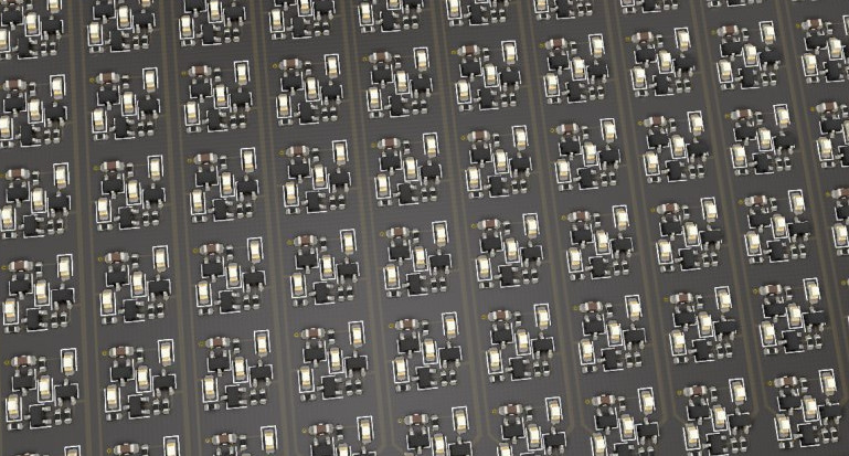
A friend of ours here at Hackaday has an audacious design in the works that we hope will one day become a prototype that we can feature here. That day may be a little while coming though, because it has somewhere close to a thousand of the smaller SMD components in multiple repeated blocks on a modestly sized board, and his quote from a Chinese board house for assembly is eye-watering. He lacks a pick-and-place machine of his own, and unsurprisingly the idea of doing the job by hand is a little daunting.

We can certainly feel his pain, for in the past we’ve been there. The job described in the linked article had a similar number of components with much more variety and on a much larger board, but still took two experienced engineers all day and into the night to populate. The solder paste had started to spread by the end, morphing from clearly defined blocks to an indistinct mush often covering more than one pad. Our eyes meanwhile were somewhat fatigued by the experience, and it’s not something any sane person would wish to repeat.

Mulling over our friend’s board and comparing it with the experience related above, are we on the edge of what is possible with hand pick-and-place, or should we be working at the next level? Board assembly is a finely judged matter of economics at a commercial level, but when at a one-off personal construction level the option of paying for assembly just isn’t there, is there a practical limit to the scale of the task? Where do you, our readers, draw the line? We’d love to hear your views.

Meanwhile our friend’s audacious project is still shrouded in a bit of secrecy, but we’ll continue to encourage him to show it to the world. It’s not often that you look at a circuit diagram and think “I wish I’d thought of that!”, but from what we’ve seen this fits the category. If he pulls it off then we’ll bring you the result.

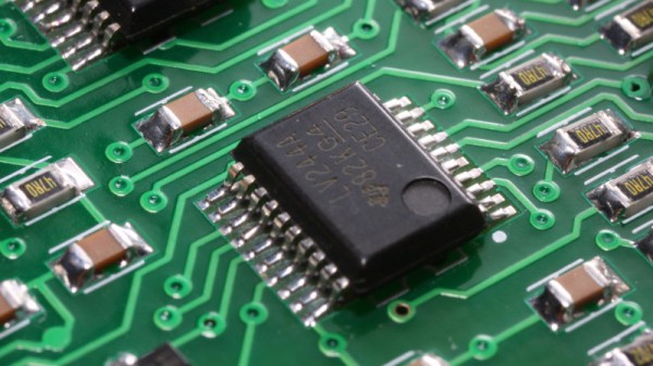
PCB image, Andrew Magill (CC BY 2.0).

Control The Suck With This Manual Vacuum Pick-And-Place Tool

The tapes that surface-mount devices come in may be optimized for automated pick and place, but woe betide those who try to dig components out manually. No matter what size package, the well on the tape seems to be just a wee bit too small to allow tweezers to grip it, so you end up picking the thing up edgewise or worse, pinching too tight and launching the tiny thing into The Void. We hope you ordered extra.

Such circumstances are why vacuum handlers were invented, but useful as they are for picking and placing SMDs, they aren’t perfect. [Steve Gardener]’s sub-optimal experience with such tools led him to build this custom vacuum pick-and-place tool. It’s based on an off-the-shelf Weller unit, of which only the handpiece remains. A bigger, more powerful vacuum pump is joined in a custom enclosure by a PCB with a PIC18F13K22 microcontroller, a power supply, a solenoid to control the vacuum, and a relay to switch the pump. A footswitch starts the pump and closes the vacuum vent; letting off the pedal opens the vent to drop the part, while the pump keeps running for a variable time. This lets him rapidly work through a series of parts without having to build vacuum back up between picks. The video below shows the build and the tool in action.

We love the idea of this tool, and the polished look is pretty slick too. If manual pick-and-place isn’t for you, though, maybe converting a 3D-printer into an automated PnP is something to check out.

Continue reading “Control The Suck With This Manual Vacuum Pick-And-Place Tool”

A Very Different ‘Hot Or Not’ Application For Your Phone

Radioactivity stirs up a lot of anxiety, partially because ionizing radiation is undetectable by any of the senses we were born with. Anytime radiation makes the news, there is a surge of people worried about their exposure levels and a lack of quick and accurate answers. Doctors are flooded with calls, detection devices become scarce, and fraudsters swoop in to make a quick buck. Recognizing the need for a better way, researchers are devising methods to measure cumulative exposure experienced by commodity surface mount resistors.

Cumulative exposure is typically tracked by wearing a dosimeter a.k.a. “radiation badge”. It is standard operating procedure for people working with nuclear material to wear them. But in the aftermath of what researchers euphemistically call “a nuclear event” there will be an urgent need to determine exposure for a large number of people who were not wearing dosimeters. Fortunately, many people today do wear personal electronics full of components made with high purity ingredients to tightly controlled tolerances. The resistor is the simplest and most common part, and we can hack a dosimeter with them.

Lab experiments established that SMD resistors will reveal their history of radiation exposure under high heat. Not to the accuracy of established dosimetry techniques, but more than good enough to differentiate people who need immediate medical attention from those who need to be monitored and, hopefully, reassure people in neither of those categories. Today’s technique is a destructive test as it requires removing resistors from the device and heating them well above their maximum temperature, but research is still ongoing in this field of knowledge we hope we’ll never need.

If you prefer to read about SMD resistor hacks with less doomsday, we recently covered their use as a 3D printer’s Z-axis touch sensor. Those who want to stay on the topic can review detection hacks like using a single diode as a Geiger counter and the IoT dosimeter submitted for the 2017 Hackaday Prize. Or we can choose to focus on the bright side of radioactivity with the good things made possible by controlled artificial radioactivity, pioneered by Irène Joliot-Curie.

[via Science News]

The Craziest Live Soldering Demo Is The Cyborg Ring

You can define the word crazy in myriad ways. Some would say using SMD resistors and QFN microcontrollers as structural elements is  crazy. Some would say hand soldering QFN is crazy, much less trying to do it on edge rather than in the orientation the footprint is designed for. And of course doing it live on stage in front of people who eat flux for breakfast is just bonkers. But Zach did it anyway and I’m delighted he did.

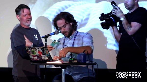
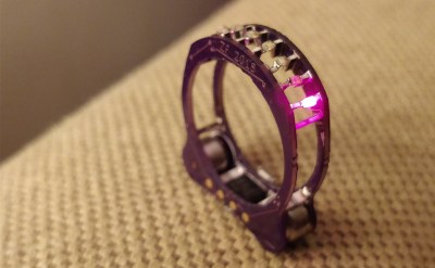
This is the cyborg ring, and it’s a one-of-a-kind leap in imagination — the kind of leap people have come to expect from Zach Fredin who modeled neurons on PCBs, depopulated an SMD LED matrix and airwired it, and replaced his ThinkPad fingerprint reader with an ARM debugger port. The construction leverages the precise nature of manufactured parts: the ATtiny85 that drives the ring is exactly twice the width of an 0805 component. This means he can bridge the two circuit boards that make up the ring with the QFN microcontroller, and then use two 10M Ohm resistors as structural spacers in a few places around the ring. The jewels in this gem of a project are red LEDs that can be addressed in an animated pattern.

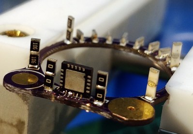
There’s an adage that all live talk demos are doomed to fail, and indeed the uC in this project doesn’t want to speak to the programmer at the end of the 9-minute exhibition. But Zach did manage to solder the two halves on the ring together live on stage, and it’s worth enduring the camera issues and low starting volume at the start of this livestream to watch him perform some crazy magic. Good on you Zach for putting yourself out there and showing everyone that there’s more than one way to stack resistors.

If this demo leaves you wanting to hear more of what Zach’s adventures, we recommend checking out his 2016 Supercon talk on the Neurobytes development and manufacturing process.

Continue reading “The Craziest Live Soldering Demo Is The Cyborg Ring”

[Leo] Repairs A MIDI Sequencer

We all have that friend who brings us their sad busted electronics. In [Leo’s] case, he had a MIDI sequencer from a musician friend. It had a dead display and the manufacturer advised that a driver IC was probably bad, even sending a replacement surface mount part.

[Leo] wasn’t convinced though. He knew that people were always pushing on the switches that were mounted on the board and he speculated that it might just be a bad solder joint. As you can see in the video below, that didn’t prove out.

The next step was to fire up a hot air gun. Instead of removing the chip, he wanted to reflow the solder anyway. He was a little worried about melting the 7-segment LEDs so he built a little foil shield to protect it. That didn’t get things working, either.

Continue reading “[Leo] Repairs A MIDI Sequencer”

Modular Feeders For SMD Component Tape

Making one of something is pretty easy, and making ten ain’t too bad. But what if you find yourself trying to make a couple of hundred of something on your home workbench? Suddenly, small timesavers start to pay dividends. For just such a situation, you may find these modular SMD tape feeders remarkably useful.

The tape feeders come in a variety of widths, to suit different size tapes. You’ve probably seen if you’ve ever ordered SMD components in quantity from Mouser, Digikey, et al. SMD components typically ship on large tape reels, which are machine fed into automated pick and place machines. However, if you’re doing it yourself in smaller quantities, having these manual tape feeders on your desk can be a huge help. Rather than having scraps of tapes scattered across the working surface, you can instead have them neatly managed at the edge of your bench, providing components as required.

The feeders are modular, so you can stack up as many as you need for a given job. Rails are provided to affix them to the relevant work surface. We’ve seen similar work before – like this 3D-printed bowl feeder for SMD parts.


Performing A Chip Transplant To Resurrect A Dead Board

[Uri Shaked] accidentally touched a GPIO pin on his 3.3 V board with a 12 V alligator clip, frying the board. Sound familiar? A replacement would have cost $60, which for him wasn’t cheap. Also, he needed it for an upcoming conference so time was of the essence. His only option was to try to fix it, which in the end involved a delicate chip transplant.

Removing the shield on the Bluetooth LE board
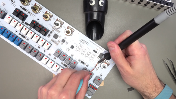
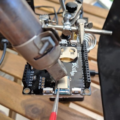
The board was the Pixl.js, an LCD board with the nRF52832 SoC with its ARM Cortex M4, RAM, flash, and Bluetooth LE. It also has a pre-installed Espruino JavaScript interpreter and of course the GPIO pins through which the damage was done.

Fortunately, he had the good instinct to feel the metal shield over the nRF52832 immediately after the event. It was hot. Applying 3.3 V to the board now also heated up the chip, confirming for him that the chip was short-circuiting. All he had to do was replace it.

Digging around, he found another nRF52832 on a different board. To our surprise, transplanting it and getting the board up and running again took only an hour, including the time to document it. If that sounds simple, it was only in the way that a skilled person makes something seem simple. It included plenty of delicate heat gun work, some soldering iron microsurgery, and persistence with a JLink debugger. But we’ll leave the details of the operation and its complications to his blog. You can see one of the steps in the video below.

It’s no surprise that [Uri] was able to dig up another board with the same nRF52832 chip. It’s a popular SoC, being used in tiny, pocket-sized robots, conference badges, and the Primo Core board along with a variety of other sensors.

Continue reading “Performing A Chip Transplant To Resurrect A Dead Board”