The Zeloof Z2 Intergrated Circuit Has 100 Transistors

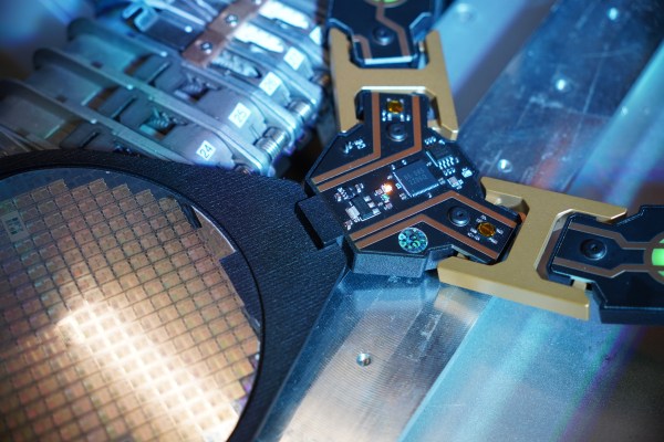
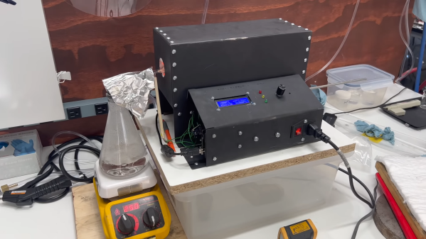
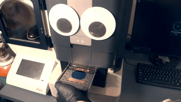
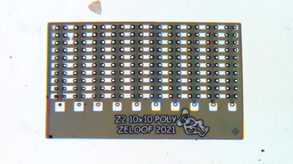
Back in 2018 we reported on the first silicon integrated circuit to be produced in a homemade chip fab. It was the work of [Sam Zeloof], and his Z1 chip was a modest six-transistor amplifier. Not one to rest on his laurels, he’s back with another chip, this time the Z2 is a hundred-transistor array. The Z2 occupies about a quarter of the area of the previous chip and uses a 10µm polysilicon gate process as opposed to the Z1’s metal gates. It won’t solve the global chip shortage, but this is a major step forward for anyone interested in building their own semiconductors.

The transistors themselves are FETs, and [Sam] is pleased with their consistency and characteristics. He’s not measured his yield on all samples, but of the twelve chips made he says he has one fully functional chip and a few others with at least 80% functionality. The surprise is that his process is less complex than one might expect, which he attributes to careful selection of a wafer pre-treated with the appropriate oxide layer.

You can see more about the Z2 in the video below the break. Meanwhile, should you wish to learn more about the Z1 you can see [Sam’s] Hackaday Superconference talk on the subject. We’re looking forward to the Z3 when it eventually arrives, with bated breath!

Continue reading “The Zeloof Z2 Intergrated Circuit Has 100 Transistors”

Superconference Interview: Sam Zeloof

In less than four days, the fifth Hackaday Superconference kicks off in Pasadena, California, and it’s shaping up to be a hoot. With a cavalcade of exciting workshops and talks on offer, hackers and makers are pouring in from across the globe for this celebration of software, firmware, and hardware.

Of course, the real gift of Supercon is the personalities which make up this awesome community. [Sam Zeloof] is one such luminary, well known for producing his very own silicon integrated circuits in his parent’s garage. Not content to keep this knowledge to himself, [Sam] gave an amazing talk at the 2018 Supercon on just what goes into creating your own silicon fab on a budget.

Our very own [Mike Szczys] caught up with [Sam] for an interview, discussing being inspired by the work of [Jeri Ellsworth], as well as the finer points of getting into lithography at home. [Sam] will be in attendance at the 2019 Superconference, of course. While he won’t be on the speaking circuit this year, his brother [Adam] will be presenting a talk called Thermodynamics for Electrical Engineers: Why Did My Board Melt (And How Can I Prevent It)?, which is sure to be a must-see.

You really should be there, but alas tickets have been sold out for almost two months! Never fear, we’ll be livestreaming the event. Be sure to subscribe to Hackaday on Youtube to be notified when it all kicks off, around 10 AM Pacific Time on Saturday, November 16th. If you scored tickets and are heading to Supercon, we can’t wait to see you there — the badge hacking begins early Friday morning.

Be sure to check out Sam’s interview after the break!

Continue reading “Superconference Interview: Sam Zeloof”

Of Roach Killer And Rust Remover: Sam Zeloof’s Garage-Made Chips

A normal life in hacking, if there is such a thing, seems to follow a predictable trajectory, at least in terms of the physical space it occupies. We generally start small, working on a few simple projects on the kitchen table, or if we start young enough, perhaps on a desk in our childhood bedroom. Time passes, our skills increase, and with them the need for space. Soon we’re claiming an unused room or a corner of the basement. Skills build on skills, gear accumulates, and before you know it, the garage is no longer a place for cars but a place for pushing back the darkness of our own ignorance and expanding our horizons into parts unknown.

It appears that Sam Zeloof’s annexation of the family garage occurred fairly early in life, and to a level that’s hard to comprehend. Sam seems to have caught the hacking bug early, and by the time high school rolled around, he was building out a remarkably well-equipped semiconductor fabrication lab at home. Sam has been posting his progress regularly on his own blog and on Twitter, and he dropped by the 2018 Superconference to give everyone a lesson on semiconductor physics and how he became the first hobbyist to produce an integrated circuit using lithographic processes.

Continue reading “Of Roach Killer And Rust Remover: Sam Zeloof’s Garage-Made Chips”

Increase Your Blinkenlights With This Silicon Wafer Necklace

Necklaces aren’t often very high-tech, mostly because of the abuse they have to go through being worn. This was obviously a problem that needed solving, so [Matt Venn] decided to change that by making a necklace out of ASICs just in time for Supercon.

Although this isn’t the first time [Matt] made such a necklace, he though his previous one was “too hip-hop” and not enough “15 million dollar Nikon Lithography Stepper”. Obviously, this means designing the whole chain, art included, from scratch with the blinkenlights to match. Together with [Pat Deegan] and [Adam Zeloof], the team created a beautiful technopunk necklace with art on every chain link and of course a real silicon wafer with a RISC-V tapeout from 2022 on it.

With [Adam] doing modeling for the chain links, and [Pat] and [Matt] designing the electronics required for the mandatory blinkenlights, and some last-minute soldering and assembling the project was finished just in time for Supercon, where it fit right in with all the other blinkenlights. It even runs on one of the RISC-V cores from the same tapeout as the central wafer!

Start Your Semiconductor Fab With This DIY Tube Furnace

Most of us are content to get our semiconductors from the usual sources, happily abstracting away the complexity locked within those little epoxy blobs. But eventually, you might get the itch to roll your own semiconductors, in which case you’ll need to start gearing up. And one of the first tools you’ll need is likely to be something like this DIY tube furnace.

For the uninitiated, [ProjectsInFlight] helpfully explains in the video below just what a tube furnace is and why you’d need one to start working with semiconductors. Perhaps unsurprisingly, a tube furnace is just a tube that gets really, really hot — like 1,200° C. In addition to the extreme heat, commercial furnaces are often set up to seal off the ends of the tube to create specific conditions within, such as an inert gas atmosphere or even a vacuum. The combination of heat and atmospheric control allows the budding fabricator to transform silicon wafers using chemical and physical processes.

[ProjectsInFlight]’s tube furnace started with a length of heat-resistant quartz glass tubing and a small tub of sodium silicate refractory cement, from the plumbing section of any home store. The tube was given a thin coat of cement and dried in a low oven before wrapping it with nichrome wire. The wrapped tube got another, thicker layer of silicate cement and an insulating wrap of alumina ceramic wool before applying power to cure everything at 1,000° C. The cured tube then went into a custom-built sheet steel enclosure with plenty of extra insulation, along with an Arduino and a solid-state relay to control the furnace. The video below concludes with testing the furnace by growing a silicon dioxide coating on a scrap of silicon wafer. This was helped along by the injection of a few whisps of water vapor while ramping the furnace temperature up, and the results are easily visible.

[ProjectsInFlight] still needs to add seals to the tube to control the atmosphere in there, an upgrade we’ll be on the lookout for. It’s already a great start, although it might take a while to catch up to our friend [Sam Zeloof].

Continue reading “Start Your Semiconductor Fab With This DIY Tube Furnace”

A wafer being loaded into an electron microscope

Using Electron Beams To Draw Tiny Shapes Onto Silicon

Over the past few years we’ve seen several impressive projects where people try to manufacture integrated circuits using hobbyist tools. One of the most complex parts of this process is lithography: the step in which shapes are drawn onto a silicon wafer. There are several ways to do this, all of them rather complicated, but [Zachary Tong] over at Breaking Taps has managed to make one of them work quite well. He shares the results of his electron-beam lithography experiments in his latest video (embedded below).

In e-beam lithography, or EBL, shapes are drawn onto a wafer using an electron beam in a vacuum chamber. This is a slow process compared to optical lithography, as used in mass production, but it is reasonably simple and very flexible. [Zach] decided to use his electron microscope as an e-beam litho machine; although not designed for lithography, it has the same basic components as a real EBL machine and can act as a substitute with a bit of software tweaking.

An AFM image of Rick Astley
[Zach] also has an atomic force microscope, which he used to make these beautiful images.
The first step is to coat a wafer with a layer of e-beam resist. [Zach] used PMMA, commonly known as acrylic plastic, and applied it using spin coating after dissolving it in anisole. He then placed the wafer into the electron microscope and used it to scan an image. The image was then developed by rinsing the wafer in cold isopropyl alcohol.

[Zach] explains the whole process in detail in his video, including how he tuned all the parameters like resist thickness, beam strength, exposure time and development time, as well as the software tricks needed to persuade the microscope to function as a litho machine. In his best runs he managed to draw lines with a width of about 100 nanometers, which is seriously impressive for such a relatively simple setup.

These e-beam lithography experiments follow on from [Zach]’s earlier research using lasers. Homebrew IC expert Sam Zeloof has also used electron beams in his work. Thanks for the tip, [smellsofbikes]!

Continue reading “Using Electron Beams To Draw Tiny Shapes Onto Silicon”

2022 Hackaday Supercon: Joe [Kingpin] Grand Keynote And Workshops Galore

It’s our great pleasure to announce that Joe [Kingpin] Grand is going to be our keynote speaker at the 2022 Supercon!

If you don’t know Joe, he’s a hacker’s hacker. He’s behind the earliest DEFCON electronic badges, to which we can trace our modern #badgelife creative culture. He was at the l0pht when it became the most publicly visible hackerspace in the USA, at the dawn of what we now think of as cybersecurity. And moreover, he’s a tireless teacher of the art of hardware hacking.

Joe’s talk at DEFCON 22 about reverse engineering PCBs on a hacker budget is on our top-10 must watch playlist, and his JTAGulator debug-port enumeration device has been present at the start of countless hacking sessions. But again, it’s his enthusiasm for creating, his inspiring “what if I poke at this thing this way?” attitude, and overwhelming hacker spirit that make Joe a long-overdue speaker at Supercon! Continue reading “2022 Hackaday Supercon: Joe [Kingpin] Grand Keynote And Workshops Galore”