2022 Hackaday Supercon: Joe [Kingpin] Grand Keynote And Workshops Galore

It’s our great pleasure to announce that Joe [Kingpin] Grand is going to be our keynote speaker at the 2022 Supercon!

If you don’t know Joe, he’s a hacker’s hacker. He’s behind the earliest DEFCON electronic badges, to which we can trace our modern #badgelife creative culture. He was at the l0pht when it became the most publicly visible hackerspace in the USA, at the dawn of what we now think of as cybersecurity. And moreover, he’s a tireless teacher of the art of hardware hacking.

Joe’s talk at DEFCON 22 about reverse engineering PCBs on a hacker budget is on our top-10 must watch playlist, and his JTAGulator debug-port enumeration device has been present at the start of countless hacking sessions. But again, it’s his enthusiasm for creating, his inspiring “what if I poke at this thing this way?” attitude, and overwhelming hacker spirit that make Joe a long-overdue speaker at Supercon! Continue reading “2022 Hackaday Supercon: Joe [Kingpin] Grand Keynote And Workshops Galore”

Integrated Circuit Manufacturing At Bell Labs In 1983

With the never ending march of technological progress, arguably the most complex technologies become so close to magic as to be impenetrable to those outside the industry in which they operate. We’ve seen walkthrough video snapshots of just a small part of the operation of modern semiconductor fabs, but let’s face it, everything you see is pretty guarded, hidden away inside large sealed boxes for environmental control reasons, among others, and it’s hard to really see what’s going on inside.

Let’s step back in time a few decades to 1983, with an interesting tour of the IC manufacturing facility at Bell Labs at Murray Hill (video, embedded below) and you can get a bit more of an idea of how the process works, albeit at a time when chips hosted mere tens of thousands of active devices, compared with the countless billions of today. This fab operates on three inch wafers, producing about 100 die each, with every one handled and processed by hand whereas modern wafers are much bigger, die often much smaller with the total die per wafer in the thousands and are never handled by a filthy human.

Particle counts of 100 per cubic foot might seem laughable by modern standards, but device geometries back then were comparatively large and the defect rate due to it was not so serious. We did chuckle somewhat seeing the operator staff all climb into their protective over suits, but open-faced with beards-a-plenty poking out into the breeze. Quite simply, full-on bunny suits were simply not necessary. Anyway, whilst the over suits were mostly for the environment, we did spot the occasional shot of an operator wearing some proper protective face shielding when performing some of the higher risk tasks, such as wafer cleaning, after all as the narrator says “these acids are strong enough to eat through the skin” and that would certainly ruin your afternoon.

No story about integrated circuit processing would be complete without mentioning the progress of [Sam Zeloof] and his DIY approach to making chips, and whilst he’s only managing device counts in the hundreds, this can only improve given time.

Continue reading “Integrated Circuit Manufacturing At Bell Labs In 1983”

OpenJewelry, No Pliers Required

They say that if you want something done right, you gotta do it yourself. Oftentimes, that goes double for getting something done at all. Whereas some people might simply lament the lack of a (stable) Thingiverse-type site for, say, jewelry designs, those people aren’t Hackaday’s own [Adam Zeloof]. With nowhere to share designs among engineering-oriented friends, [Adam] took the initiative and created OpenJewelry, a site for posting open-source jewelry and wearable art designs as well as knowledge about techniques, materials, and processes.

[Adam] has seeded the site with a handful of his own beautiful designs, which run the gamut from traditional silversmithing techniques to 3D printing to fancy PCBs with working blinkenlights. You really should check it out, and definitely consider contributing.

Even if you don’t have any jewelry designs to share, the code is open as well, or you could even edit the wiki. Just be sure to read through the contribution guidelines first. If you don’t have the time for any of that, donations are welcome as well to help maintain the site.

We love wearable art around here, especially when it serves another purpose like this UV-sensing talisman, or this air quality necklace.

Hackaday Links Column Banner

Hackaday Links: January 23, 2022

When Tonga’s Hunga-Tonga Hunga-Ha’apai volcano erupted on January 15, one hacker in the UK knew just what to do. Sandy Macdonald from York quickly cobbled together a Raspberry Pi and a pressure/humidity sensor board and added a little code to create a recording barometer. The idea was to see if the shock wave from the eruption would be detectable over 16,000 km away — and surprise, surprise, it was! It took more than 14 hours to reach Sandy’s impromptu recording station, but the data clearly show a rapid pulse of increasing pressure as the shockwave approached, and a decreased pressure as it passed. What’s more, the shock wave that traveled the “other way” around the planet was detectable too, about seven hours after the first event. In fact, data gathered through the 19th clearly show three full passes of the shockwaves. We just find this fascinating, and applaud Sandy for the presence of mind to throw this together when news of the eruption came out.

Good news for professional astronomers and others with eyes turned skyward — it seems like the ever-expanding Starlink satellite constellation isn’t going to kill ground-based observation. At least that’s the conclusion of a team using the Zwicky Transient Facility (ZTF) at the Palomar Observatory outside San Diego. ZTF is designed to catalog anything that blinks, flashes, or explodes in the night sky, making it perfect to detect the streaks from the 1,800-odd Starlink satellites currently in orbit. They analyzed the number of satellite transients captured in ZTF images, and found that fully 20 percent of images show streaks now, as opposed to 0.5 percent back in 2019 when the constellation was much smaller. They conclude that at the 10,000 satellite full build-out, essentially every ZTF image will have a streak in it, but since the artifacts are tiny and well-characterized, they really won’t hinder the science to any appreciable degree.

Speaking of space, we finally have a bit of insight into the causes of space anemia. The 10% to 12% decrease in red blood cells in astronauts during their first ten days in space has been well known since the dawn of the Space Age, but the causes had never really been clear. It was assumed that the anemia was a result of the shifting of fluids in microgravity, but nobody really knew for sure until doing a six-month study on fourteen ISS astronauts. They used exhaled carbon monoxide as a proxy for the destruction of red blood cells (RBCs) — one molecule of CO is liberated for each hemoglobin molecule that’s destroyed — and found that the destruction of RBCs is a primary effect of being in space. Luckily, there appears to be a limit to how many RBCs are lost in space, so the astronauts didn’t suffer from complications of severe anemia while in space. Once they came back to gravity, the anemia reversed, albeit slowly and with up to a year of measurable changes to their blood.

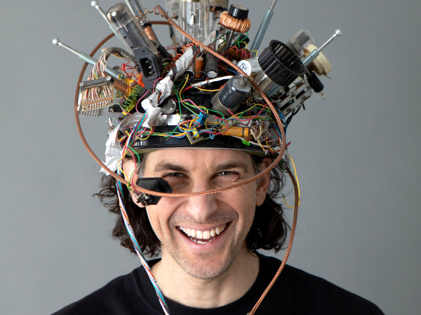
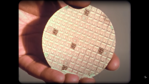
From the “Better Late Than Never” department, we see that this week that Wired finally featured Hackaday Superfriend Sam Zeloof and his homemade integrated circuits. We’re glad to see Sam get coverage — the story was also picked up by Ars Technica — but it’s clear that nobody at either outfit reads Hackaday, since we’ve been featuring Sam since we first heard about his garage fab in 2017. That was back when Sam was still “just” making transistors; since then, we’ve featured some of his lab upgrades, watched him delve into electron beam lithography, and broke the story on his first legit integrated circuit. Along the way, we managed to coax him out to Supercon in 2019 where he gave both a talk and an interview.

And finally, if you’re in the mood for a contest, why not check out WIZNet’s Ethernet HAT contest? The idea is to explore what a Raspberry Pi Pico with Ethernet attached is good for. WIZNet has two flavors of board: one is an Ethernet HAT for the Pico, while the other is as RP2040 with built-in Ethernet. The good news is, if you submit an idea, they’ll send you a board for free. We love it when someone from the Hackaday community wins a contest, so if you enter, be sure to let us know. And hurry — submissions close January 31.

Laser doping silicon wafer

Laser Doping His Way To Homemade Silicon Chips

It’s a pity that more electronics enthusiasts haven’t taken the hobby to its ultimate level: making your own semiconductors. There are plenty of good reasons for that: chief among them is the huge expense involved in obtaining the necessary equipment. But for the sufficiently clever, there are ways around that.

[Zachary Tong] is dipping his toes into the DIY semiconductor world, and further to the goal of keeping costs to a hobbyist scale, is experimenting with laser doping of silicon. Doping is the process of adding impurities to silicon wafers in a controlled manner to alter the electrical properties of the semiconductor. [Zach]’s doping method is a more localized version of the simple thermal diffusion method, which drives a dopant like phosphorus into silicon using high temperatures, but instead of using a tube furnace, he’s using a fiber laser.

The video below shows his two-step process, which first blasts the silicon oxide layer off the wafer before doping with the laser shining through a bath of phosphoric acid. The process is admittedly fussy, and the results were mixed at best. [Zach]’s testing seems to suggest that some doping occurred, and it even looks like he managed to make something reasonably diode-like using the method.

Although the jury is still out on [Zach]’s method, we thought the effort was the important bit here. Granted, not everyone has a fiber laser kicking around to replicate his results, but it’s always good to see progress in the DIY semiconductor field. Here’s hoping [Zach]’s work, along with the stuff that [Sam Zeloof] is doing, kicks off a spate of garage semiconductor fabs.

Continue reading “Laser Doping His Way To Homemade Silicon Chips”

A 1971 Thermos compliments this mid-century corner of my office.

The Incredible Tech Of The Vacuum-Seal Flask

I recently started using a 50-year-old vacuum-seal flask that belonged to my Grandpa so that I don’t have to leave the dungeon as often to procure more caffeine. Besides looking totally awesome on my side desk, this thing still works like new, at least as far as I can tell — it’s older than I am.

Sir James Dewar's original vacuum-seal flask.
Sir James Dewar’s original vacuum-seal flask. Image via the Royal Institute

Of course this got me to wondering how exactly vacuum-seal flasks, better known in household circles as Thermoses work, and how they were invented. The vacuum-seal flask is surprisingly old technology. It was first invented by Scottish chemist Sir James Dewar and presented to the Royal Institute in 1892. Six years later, he would be the first person to liquefy hydrogen and is considered a founding father of cryogenics. Continue reading “The Incredible Tech Of The Vacuum-Seal Flask”

Scanning electron micrograph of a microfabricated lens array

Getting A Fly’s-Eye View With Microfabricated Lens Arrays

Atomic force microscopy, laser ablation, and etching with a witches brew of toxic chemicals: sounds like [Zachary Tong] has been playing in the lab again, and this time he found a way to fabricate arrays of microscopic lenses as a result.

Like many of the best projects, [Zach]’s journey into micro-fabrication started with a happy accident. It happened while he was working on metal-activated chemical etching (MACE), which uses a noble metal catalyst to selectively carve high-aspect-ratio features in silicon. After blasting at a silver-coated silicon wafer with a laser, he noticed the ablation pits were very smooth and uniform after etching. This led him to several hypotheses about what was going on, all of which he was able to test.

The experiments themselves are pretty interesting, but what’s really cool is that [Zach] realized the smooth hemispherical pits in the silicon could act as a mold for an array of microscopic convex lenses. He was able to deposit a small amount of clear silicone resin into the mold by spin-coating, and (eventually) transfer the microlens array to a glass slide. The lenses are impressively small — hundreds of them over only a couple hundred square microns — and pretty well-formed. There’s always room for improvement, of course, but for an initial attempt based on a serendipitous finding, we’d call it a win. As for what good these lenses are, your guess is as good as ours. But novel processes like these tend to find a way to be useful, and the fact that this is coming out of a home lab doesn’t change that fact.

We find this kind of micro-fabrication fascinating. Whether it’s making OLED displays, micro-machining glass with plasma, or even rolling your own semiconductors, we can’t get enough of this stuff.

Continue reading “Getting A Fly’s-Eye View With Microfabricated Lens Arrays”