We all have our shiny, modern computers for interacting with the modern world, but at times they can seem a little monochromatic. Even the differences between something like macOS and Windows for the average user often boil down to which operating system loads an Internet browser. There are obviously more differences than that, but back in the 80s it was much more extreme with interoperability a pipe dream in most cases. What keeps drawing people to maintaining and using computers from that chaotic era is more tangible compared to modern machines, and that is meant quite literally; computers from this era can be saved from an extreme amount of degradation like this Commodore that was nearly completely destroyed before it was re-discovered.
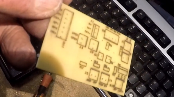
The first step was to restore the case of this Commodore PC20-III, but the restoration of the computer’s internals took a bit more time. First, the entire board was de-soldered, with any rare chips being set aside for future use. Unfortunately the board itself was too corroded and otherwise damaged to be used, but since these were just two-layer boards it could be photographed and then re-created in CAD software to make a near-perfect duplicate of the original. The team at [The Cave] took the opportunity to add patch wires which would have been present in the original machine into the PCB, and made some other upgrades as well like adding sockets to various chips that would have been originally soldered to the board.
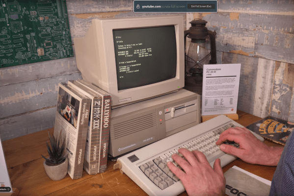
The passive components, especially capacitors, were brand new as well and some period-correct components such as a monitor and keyboard finish out the build. The computer boots on the first try, and is quickly put through its paces testing the hard disk drive, using the old floppy drive, and even playing a few video games from the era. The fact that retrocomputers like these are easy (by modern standards) to reverse engineer and restore surely leads to their continued popularity, and we’ve seen everything from C64s to this 128DCR get a similar full restoration.