There’s a piece of tech that many of us own, but very few of us have dissected. This is strange, given our community’s propensity for wielding the screwdriver, but how many of you have taken apart a camera lens. Even though many of us have a decent camera, almost none of us will have taken a lens to pieces because let’s face it, camera lenses are expensive!
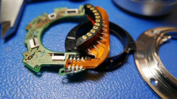
[Anthony Kouttron] has taken that particular plunge though, because in cleaning his Olympus lens he tore its internal ribbon cable from the camera connector to the PCB. Modern lenses are not merely optics in a metal tube, their autofocus systems are masterpieces of miniaturised electronics that penetrate the entire assembly.
In normal circumstances this would turn the lens from a valued photographic accessory into so much junk, but his solution was to take the bold path of re-creating the torn cable in KiCad and have it made as a flexible PCB, and to carefully solder it back on to both connector and autofocus PCB. We applaud both the quality of his work, and thank him for the unusual glimpse into a modern lens system.
Lens repairs may be thin on the ground here, but we’ve had another in 2015 with this Nikon aperture fix.
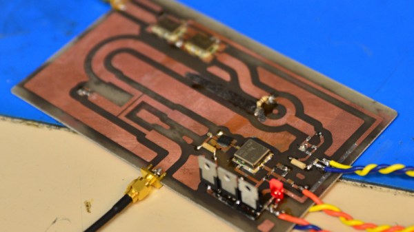
If you’ve ever cast your eyes towards experimenting with microwave frequencies it’s likely that one of your first ports of call was a cheaply-available Doppler radar module. These devices usually operate in the 10 GHz band, and the older ones used a pair of die-cast waveguide cavities while the newer ones use a dielectric resonator and oscillator on a PCB. If you have made your own then you are part of a very select group indeed, as is [Reed Foster] and his two friends who made a Doppler radar module their final project for MIT’s 6.013 Applications of Electromagnetics course.
Their module runs at 2.4 GHz and makes extensive use of the notoriously dark art of PCB striplines, and their write-up offers a fascinating glimpse into the world of this type of design. We see their coupler and mixer prototypes before they combined all parts of the system into a single PCB, and we follow their minor disasters as their original aim of a frequency modulated CW radar is downgraded to a Doppler design. If you’ve never worked with this type of circuitry before than it makes for an interesting read.
We’ve shown you a variety of commercial Doppler modules over the years, of which this teardown is a representative example.
The artistic elite exists in a stratum above we hoi polloi, a world of achingly trendy galleries, well-heeled collectors, and art critics who act as gatekeepers to what is considered the pinnacle du jour of culture. Artistic movements that evolve outside this bubble may be derided or ignored as naive and unsophisticated, even in complete denial of their raw creative edge. When they are discovered by the establishment a few of their artists are selected and anointed, while inevitably the crucible in which they were formed is forgotten. On the streets of Bristol the incredible work of far more graffiti artists can be seen than just that of Banksy.
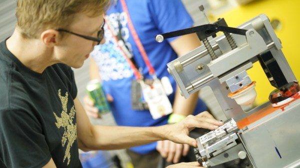
Our community has an art form all of its own, in the guise of PCB artwork and the #BadgeLife community. One day you will see electronic badges from darlings of the art world behind glass in those trendy galleries, but for now they live in glorious abundance in the wild. Here at Hackaday we are lucky enough to have in Brian Benchoff a colleague who is pushing the boundaries of PCB art, and at the Hackaday Superconference he took us through one of his more recent pieces of work.
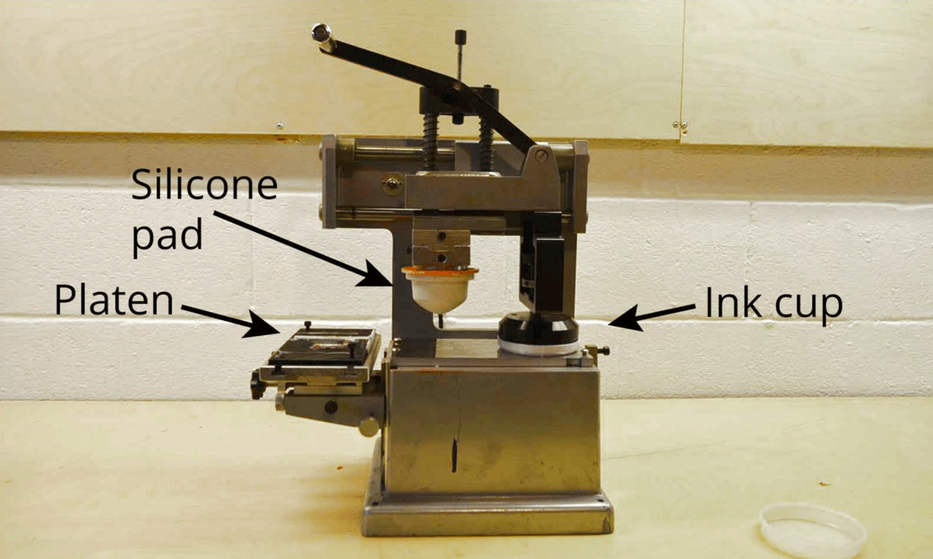
Brian’s pad printer.
The colour palette of a typical printed circuit board is limited by the combination of fibreglass, copper, soldermask, plating, and silkscreen its designer selects. Thus while the variety of soldermask colours and plating materials can make for an eye-catching work, they have remained a colour-tinted near monochrome. The Holy Grail of the PCB artist has been to step into the world of full colour, and Brian has been pursuing that goal by exploring pad printing to produce extra colours beyond the sodermask..
It’s a subject he’s written about here in the past, and he introduces it in the talk with a look at existing badge artwork and a mention of an expensive commercial inkjet process before considering the type of printing you see daily on the sides of promotional pens. Those company titles are deposited on pens using pad printing, an offset process in which ink is first deposited upon a photo-etched metal plate before being picked up on a silicone rubber pad for transfer to the object to be printed. It’s not the panacea for all coloured-PCB tasks, but for adding relatively small blocks of pigment to an otherwise monochromatic board it can be very successful.
The eye-catching Kiss -themed Tindie badges.
Brian’s examples are a panelised set of Tindie badges as a homage to the rock band Kiss, and his Tide pod addon containing a serial number in an EEPROM that was part of a Blockchain-inspired game. The Kiss Tindie badges use black soldermask with extensive white silkscreen and a modest area of red pad printing for the stage makeup, while the Tide addon makes clever use of the same swoosh printed in alternate colours at 180 degrees to each other.
In both cases there is some labour involved in creating the prints, and as his detailed write-up of printing the Tide pods reminds us, the process of creating the printing plate is not exactly an easy one. But it remains the best way yet to add extra colours to a board without paying a small fortune for the inkjet process, and if you’d like to put your own designs at the bleeding edge of PCB art you might wish to read his writeups and watch the video below the break.
This is just one example of the kind of manufacturing techniques, and electronic design principles on display at the Hackaday Superconference. There’s another Supercon just around the corner, so grab your ticket and send in your own talk proposal right away!
We take the everyday materials of engineering for granted, as ubiquitous components rather than as complex items in their own right. Sure, we know that an integrated circuit represents the pinnacle of a hundred years’ development in the field of electronics, but to us it’s simply a black box with some wires. Even with more basic materials it’s easy to forget the work that goes into their manufacture, as for example with the two videos below the break. They both take a look from a very different angle at the creation of the same product: metal chain. However, the approaches couldn’t be more different as the two examples are separated by about a century and with vastly different techniques and material.
The first film follows the manufacture of the chain and anchor that would have been found on a ship around the turn of the twentieth century. One of the text frames mentions Netherton Works, allowing us to identify it as being filmed at N. Hingley & Sons, a specialist anchor and chain manufacturer based in the area to the west of the English city of Birmingham known as the Black Country. It’s a window on a manufacturing world that has entirely disappeared, as large gangs of men do almost every task in the process by hand, with very few automated steps. There is scant regard for health and safety in handling the huge pieces of red-hot metal, and the material in question is not the steel we’d be used to today but wrought iron. The skill required to perform some of the steps such as forge-welding large anchor parts under a steam hammer is very significant, and the film alone can not convey it. More recent videos of similar scenes in Chinese factories do a better job.
The other video is contemporary, a How It’s Made look at chain manufacture. Here the chains involved are much smaller, everything is done by automated machinery, and once we have got over marveling at the intricacy of the process we can see that there is far more emphasis on the metallurgy. The wire is hard drawn before the chain is formed, and then hardened and annealed in a continuous process by a pair of induction heaters and water baths. I’m trying really hard to avoid a minor rant about the propensity of mass-market entertainment such as this for glossing over parts of the process. A keen eye notices that each link has become welded but we are not shown the machine that performs the task.
Most of us will never have the chance of a peek into a chain factory, so the medium of YouTube industrial films and videos is compulsive viewing. These two views of what is essentially the same process could not be more different, however it would be wrong to assume that one has replaced the other. There would have been mechanised production of small chains when the first film was made, and large chains will still be made today with fewer workers and from arc-welded steel rather than wrought iron. Plants like the Hingley one in Netherton may have closed in the 1980s, but there is still a demand for chains and anchors.
There are plenty of techniques and components that we use in our everyday hardware work, for which their connection and coding is almost a done deal. We are familiar with them and have used them before, so we drop them in without a second thought. But what about the first time we used them, we had to learn somewhere, right? [TheMagicSmoke] has produced just what we’d have needed then for one component that’s ubiquitous, the I2C EEPROM.
These chips provide relatively small quantities of non-volatile memory storage, and though they are not the fastest of memory technologies they have a ready application in holding configuration or other often-read and rarely written data.
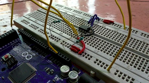
Since the ST24C04 512-byte device in question has an I2C bus it’s a straightforward add-on for an Arduino Mega, so we’re shown the wiring for which only a couple of pull-down resistors are required, and some sample code. It’s not the most complex of projects, but it succinctly shows what you need to do so that you too can incorporate an EEPROM in your work.
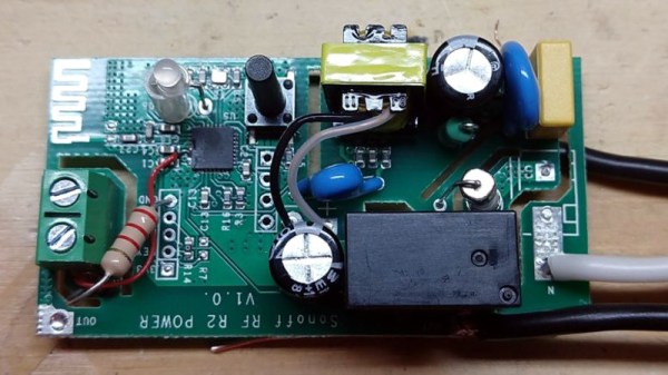
Underfloor heating is a wonderfully luxurious touch for a bedroom and en-suite bathroom, and [Andy] had it fitted so that he could experience the joy of walking on a toasty-warm floor in the morning. Unfortunately after about a year it stopped working and the culprit proved to be its thermostat. A replacement was eye-wateringly expensive, so he produced his own using an ESP8266-powered Sonoff wireless switch.
The thermostat has a thermistor as its temperature sensor, embedded in the floor itself. This could be brought to the ESP’s solitary ADC pin, but not without a few challenges along the way. The Sonoff doesn’t expose the pin, so some very fine soldering was the first requirement. A simple voltage divider allowed the pin to be fed, but through it he made the unfortunate discovery that the ESP’s analogue input has a surprisingly low voltage range. A new divider tying it to ground solved the problem, and he was good to go.
Rather than using an off-the-shelf firmware he created his own, and with a bit of board hacking he was able to hard wire the mains cabling and use one set of Sonoff terminals as a sensor connector. The whole fit neatly inside an electrical fitting box, so he’s back once more to toasty-warm feet.
This year we’ve added something new and exciting to the Hackaday Prize mix. Mentor sessions link up hardware teams with experts from backgrounds useful in moving their product development forward. We’ve assembled a dream team of mentors, and today we’re excited to publish video of the first mentor session which you’ll find embedded below. It’s a great chance to hear about the engineering going into each entry, and to learn from these back and forth conversations that help move the effort forward. We encourage you to sign up for an upcoming session!
Giovanni Salinas, the Product Development Engineer at Supplyframe’s DesignLab, is the mentor for this session. He has a huge breadth of experience in product development, and in today’s installment he’s working with four different product teams.


 The first film follows the manufacture of the chain and anchor that would have been found on a ship around the turn of the twentieth century. One of the text frames mentions Netherton Works, allowing us to identify it as being filmed at
 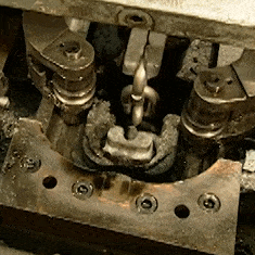 The other video is contemporary, a How It’s Made look at chain manufacture. Here the chains involved are much smaller, everything is done by automated machinery, and once we have got over marveling at the intricacy of the process we can see that there is far more emphasis on the metallurgy. The wire is hard drawn before the chain is formed, and then hardened and annealed in a continuous process by a pair of induction heaters and water baths. I’m trying really hard to avoid a minor rant about the propensity of mass-market entertainment such as this for glossing over parts of the process. A keen eye notices that each link has become welded but we are not shown the machine that performs the task.