This excellent content from the Hackaday writing crew highlights recurring topics and popular series like Linux-Fu, 3D-Printering, Hackaday Links, This Week in Security, Inputs of Interest, Profiles in Science, Retrotechtacular, Ask Hackaday, Teardowns, Reviews, and many more.
The Raspberry Pi Zero was announced this week, so you know what that means: someone is going to destroy a Game Boy Micro. If you’re interested in putting the Zero in a tiny handheld of your own design, here are the dimensions, courtesy of [Bert].
There are a lot — a lot — of ‘intro to FPGA’ boards out there, and the huge variety is an example of how the ‘educational FPGA’ is a hard nut to crack. Here’s the latest one from a Kickstarter. It uses an ICE40, so an open source toolchain is available, and at only $50, it’s cheap enough to start digging around with LUTs and gates.
Over on Hackaday.io, [Joseph] is building a YAG laser. This laser will require a parabolic mirror with the YAG rod at the focus. There’s an interesting way to make one of these: cut out some acrylic and beat a copper pipe against a form. A little polish and nickel plating and you have a custom mirror for a laser.
[David Windestål] is awesome. Completely and totally awesome. Usually, he’s behind the controls of an RC plane or tricopter, but this time he’s behind a slo-mo camera, an RC heli, and a watermelon. That’s a 550-sized heli with carbon fiber blades spinning at 2500 RPM, shot at 1000 FPS.
“If I could save time in a bottle…” it’s not just an old song, it’s a passion for many photography hackers. Time-lapse photography is a way to show the movement of time through still images. These images are animated into what essentially is a video recorded at a super low frame rate. We’re talking one frame per minute or slower in some cases! The camera doesn’t have to be still for all this, but any motion must be carefully controlled. This has led hackers, makers, and engineers to create a myriad of time-lapse rigs. This week’s Hacklet is all about some of the best time lapse projects on Hackaday.io!
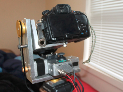
We start with [Swisswilson] and the simply named Timelapse rig. To say this rig is beefy would be an understatement. All the aluminum parts, with the exception of the gears, were machined by [Swisswilson]. Two Nema-23 Nema-17 motors are controlled by Sparkfun Easy Stepper Drive boards, while an Arduino Micro serves as the controller. The electronics are all housed in a sturdy box which also serves as a remote control. A joystick allows pan and tilt to be manually controlled. The bombproof construction is definitely a help here, as [Swisswilson] is using this rig with DSLR cameras. Combined with a lens, these setups can reach a pound or two.
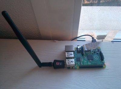
Next up is [minWi], who put their script-foo to work with raspilapse. Raspilapse automates the entire process of taking photos, assembling them into a movie, and uploading to YouTube. The hardware is a Raspberry Pi Model B, with a RasPi Camera. The Pi shoots images then uploads them to a Virtual Private Server (VPS). [minWi] used an external server to save wear and tear on the Pi’s SD storage card. At the end of the day, the VPS uses ffmpeg to assemble the images into a video, then uploads the whole thing to YouTube. We’re betting that with a few script mods, this entire process could be run on a Raspberry Pi 2. If you’re really worried about the SD card, a USB flash drive could be used.
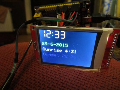
[Andyhull] takes us down to one frame per day with Sunset and Sunrise camera controller. [Andy] wanted to get shots of the sunrise every day. Once converted to a video, these shots are great for documenting the passing of the seasons. He used a Canon point and shoot camera along with the Canon Hack Devleoper’s Kit (CHDK) for his camera. The camera has its own real-time clock, and with CHDK, it can be programmed to shoot images at sunrise. The problem is power. Leaving the camera on all the time would quickly drain the batteries. Arduino to the rescue! [Andy] programmed an Arduino Pro Mini to turn the camera on just before sunrise, then shut it back down. The standby power of a sleeping ATmega328 is much lower than the camera’s, leading to battery life measured in weeks.
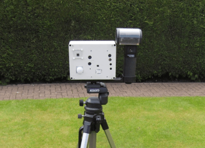
Finally, we have [caramellcube] who added data to their time-lapse photos with Portable Observation Device (POD). POD was conceived as a device to aid paranormal investigators. The idea was to have a device that could take images and record data at a set interval from within a locked room. Sounds like a job for a Raspberry Pi! [caramellcube] started with Adafruit’s Raspberry Pi-based touchscreen camera kit. From there they added a second board controlled by an Arduino Nano. The Nano reads just about every sensor [caramellcube] could fit, including humidity, air pressure, magnetic field strength, acceleration, light (4 bands), sound, and static charge. The Nano allows [caramellcube] to connect all those sensors with a single USB port on the Pi. We’re not sure if [caramellcube] has found any ghosts, but we’re sure our readers can think of plenty of uses for a device like this!
If you want to see more time-lapse projects, check out our new time-lapse projects list! If I missed your project, don’t be shy, just drop me a message on Hackaday.io. That’s it for this week’s Hacklet. As always, see you next week. Same hack time, same hack channel, bringing you the best of Hackaday.io!
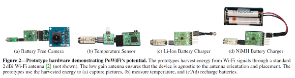
There have been a few reports of power over WiFi (PoWiFi) on the intertubes lately. If this is a real thing it’s definitely going to blow all of the IoT fanboys skirts up (sorry to the rest of you *buzzword* fanboys, the IoT kids flash-mobbed the scene and they mean business).
All of the recent information we found points to an article by [Popular Science] titled “Best of What’s New 2015”. The brief write up includes a short summary lacking technical info, and fair play to [PopSci] as it’s a “Best Of” list for which they hadn’t advertised as an in-depth investigation.
However, we tend to live by the “If you’re gonna get wet, you might as well swim.” mentality, so we decided to get a little more information on the subject. After a bit of digging around we came across the actual article on [Cornell University]’s e-print archive where you can download the PDF that was published.
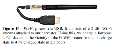
USB energy harvesting dongle.
The paper goes into detailed explanation of the power harvesting theory including a schematic of the receiving end hardware. They had to create a constant transmission for the harvester to get over its minimum required voltage of operation. This was done with one of the wireless router’s unused channels to fill the voids of packet-less silence between normal WiFi communication.
As you can imagine PoWiFi is currently limited to powering/charging very low power devices that are used intermittently. The research team was able to charge a Jawbone headset at a rate of 2.3mA for 2.5 hours which resulted in the battery going from 0-41%. The punchline here is the distance, the device being charged was only 5-7cm from the PoWiFi router which is getting close to inductive charging range. The researchers stated in the paper that they were looking into integrating the harvesting circuitry and antenna into the headset while working towards a larger charging distance.
Rate of update vs time.
WiFi packets and silence.
Power harvesting schematic.
At the time of writing this article it seems that PoWiFi is best suited for devices such as: low powered sensors and motion activated cameras that have increased energy storage capacity, which the team mentioned as one of the continued research possibilities.
We’ve covered numerous wireless power projects before, some legit and some we still get a kick out of. Where do you think this one falls on that spectrum? Let us know in the comments below.
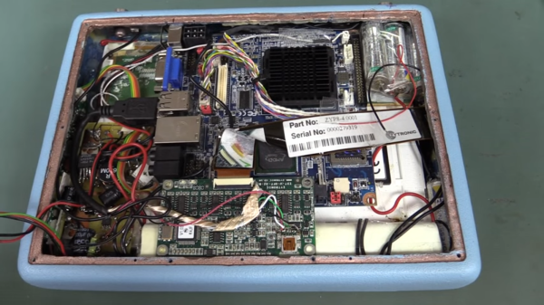
Nothing spices up a quiet afternoon like the righteous indignance of an upset engineer, especially if that engineer is none other than [Dave Jones], on his EEVblog YouTube Channel. This week [Dave] has good reason to be upset. A viewer sent him what looked to be a nondescript 2010 era tablet from a company called Esinomed. From the outside it looked like a standard issue medical device. Opening up the back panel tells a completely different story though. This thing is quite possibly the worst hack job [Dave] (and we) have ever seen. This is obviously some kind of sales demo or trade show model. Even with that in mind, this thing is a fail.
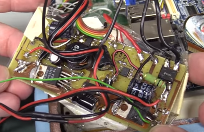
The tablet is based upon an off-the-shelf embedded PC motherboard and touchscreen controller. [Dave] took some offense at the hacked up USB connector on the touchscreen. We have to disagree with [Dave] a bit here, as the video seems to show that a standard mini-b connector wouldn’t have fit inside the tablet’s case. There’s no excuse for the USB cable shield draped over the bare touch controller board though. Things go downhill from there. The tablet’s power supply is best described as a bizarre mess. Rather than use a premade DC to DC converter, whoever built this spun their own switch mode power supply on a home etched board. The etching job looks good, but everything else, including the solder job, is beyond terrible. All the jumps and oddly placed components make it look like a random board from the junk bin was used to build this supply.
The story gets even worse with the batteries. The tablet has horribly hand soldered NiMH cells shoved here, there and everywhere. Most of the cells show split shrink wrap – a sure sign they have been overheated. It’s hard to tell from the video, but it appears as if a few cells have their top mounted vent holes covered with solder. That’s a great way to turn a simple rechargeable battery into a pipe bomb. Batteries can be safely hand soldered – Radio Controlled modelers did it for decades before LiPo cells took over.
We’ve all hacked projects together at the last minute; that’s one of the things we celebrate here on Hackaday. However, since this is a commercial medical device (with serial number 11 no less) we have to stamp this one as a fail.
Imagine that you’re coordinating a large scale search-and-rescue mission in a cave. You need to know where all your groups are, and whether or not they’ve found anything. But how do they all communicate to the command center?
You’d guess radio, but you’d guess wrong. Radio doesn’t propagate well at all in a maze of twisty passages, all alike; rocks absorb radio waves, especially in the VHF/UHF range that’s best suited for most small radios. In the past, you’d run wire and transmit along it. This article runs through the options in detail. But adding miles of wire to your already heavy caving and climbing gear is a nuisance or worse.
Last week, the Nvidia Jetson TX1 was released. This credit card-sized module is a ‘supercomputer’ advertised as having more processing power than the latest Intel Core i7s, while running at under 10 Watts. This is supposedly the device that will power the next generation of things, using technologies unheard of in the embedded world.
A modern day smartphone could have been built 10 or 15 years ago. There’s no question the processing power was there with laptop CPUs, and the tiny mechanical hard drives in the original iPod was more than spacious enough to hold a library of Napster’d MP3s and all your phone contacts. The battery for this sesquidecadal smartphone, on the other hand, was impossible. The future depends on batteries and consequently low power computing. Is the Jetson TX1 the board that will deliver us into the future? It took a hands-on look to find out.
The Nvidia Jetson TX1 and Carrier Board
What is the TX1
The Jetson TX1 is a tiny module – 50x87mm – encased in a heat sink that brings the volume to about the same size as a pack of cigarettes. Underneath a block of aluminum is an Nvidia Tegra X1, a module that combines a 64-bit quad-core ARM Cortex-A57 CPU with a 256-core Maxwell GPU. The module is equipped with 4GB of LPDDR4-3200, 16GB of eMMC Flash, 802.11ac WiFi, and Bluetooth.
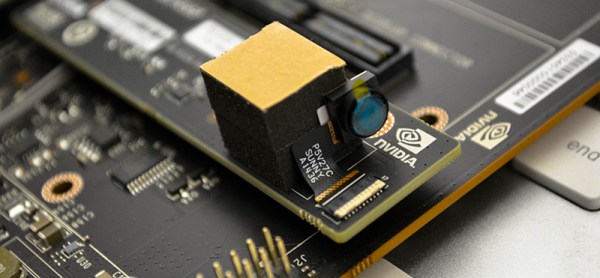
This module connects to the outside world through a 400-pin connector (from Samtec, a company quite liberal with product samples, by the way) that provides six CSI outputs for a half-dozen Raspberry Pi-style cameras, two DSI outputs, 1 eDP 1.4, 1 eDP 1.2, and HDMI 2.0 for displays. Storage is provided through either SD cards or SATA. Other ports include three USB 3.0, three USB 2.0, Gigabit Ethernet, a PCIe x1 and PCIe x4, and a host of GPIOs, UARTs, SPI and I2C busses.
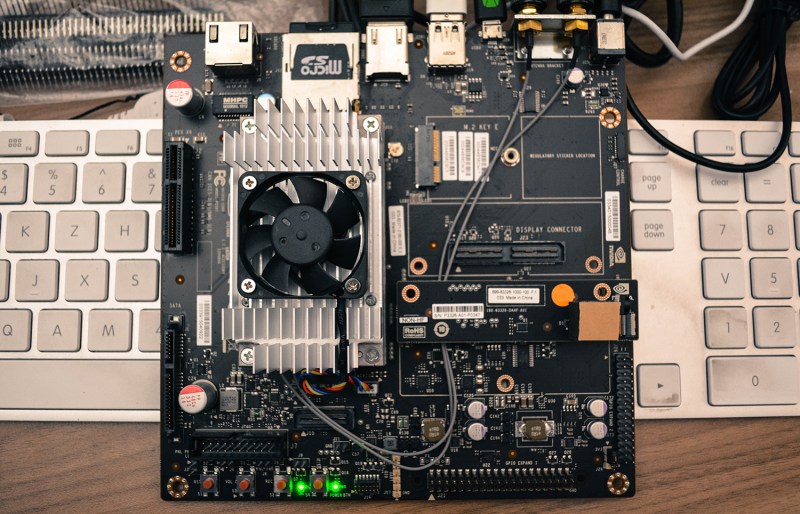
The only way of getting at all these extra ports is, at the moment, the Jetson TX1 carrier board, a board that is effectively a MiniITX motherboard. Mount this carrier board in a case, modify a power supply and figure out how to wire up the front panel buttons, and you’ll have a respectable desktop computer.
This is not a desktop computer, though, and it’s not a replacement for a Raspberry Pi or Beaglebone. This is an engineering tool – a device built to handle the advanced robotics work of the future.
Benchmarks
No tech review would be complete without benchmarks, and since this is an Nvidia board, that means a deep dive into the graphics performance.
The review unit Nvidia sent over came with an incredible amount of documentation, pointing me towards GFXBench 4.0 Manhattan 3.1 (and the T-rex one) to test the graphics performance.
In terms of graphics performance, the TX1 isn’t that much different from a run-of-the-mill mobile chipset from a few years ago. This is to be expected; it’s unreasonable to expect Nvidia to put a Titan in a 10 Watt module; the Titan itself sucks up about 250 Watts.
What about CPU performance? The ARM Cortex A57 isn’t seen very much in tiny credit-card sized dev boards, but there are a few actual products out there with it. The TX1 isn’t a powerhouse by any means, but it does trounce the Raspberry Pi 2 Model B in testing by a factor of about three.
Compared to desktop/x86 performance, the best benchmarks again put the Nvidia TX1 in the same territory as a middling desktop from a few years ago. Still, that desktop probably draws about 300 W total, where the TX1 sips a meager 10 W.
This is not the board you want if you’re mining Bitcoins, and it’s not the board you should use if you need a powerful, portable device that can connect to anything. It’s for custom designs. The Nvidia TX1 is a module that’s meant to be integrated into products. It’s not a board for ‘makers’ and it’s not designed to be. It’s a board for engineers that need enough power in a reasonably small package that doesn’t drain batteries.
With an ARM Cortex A57 quad core running at almost 2 GHz, 4 GB of RAM, and a reasonably powerful graphics card for the power budget, the Nvidia TX1 is far beyond the usual tiny Linux boards. It’s far beyond the Raspi, the newest Beagleboard, and gives the Intel NUC boards a run for their money.
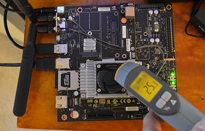
That huge and heavy heatsink is useful; while benchmarking the TX1, temperatures were only one or two degrees above ambient
In terms of absolute power, the TX1 is about as powerful as a entry-level laptop from three or four years ago.
The Jetson TX1 is all about performance per Watt. That’s exceptional, new, and exciting; it’s something that simply hasn’t been done before. If you believe the reams of technical documents Nvidia granted me access to, it’s the first step to a world of truly smart embedded devices that have a grasp on computer vision, machine learning, and a bunch of other stuff that hasn’t really found its way into the embedded world yet.
Alexnex images processed per second per Watt. No, Joules do not exist.
And here lies the problem with the Jetson TX1; because a platform like this hasn’t been available before, the development stack, examples, and community of users simply isn’t there yet. The number of people contributing to the Nvidia embedded systems forum is tiny – our Hackaday articles get more comments than a thread on the Nvidia forums. Like all new platforms, the only thing missing is the community, putting Nvidia in a chicken and egg scenario.
This a platform for engineers. Specifically, engineers who are building autonomous golf carts and cars, quadcopters that follow you around, and robots that could pass a Turing test for at least 30 seconds. It’s an incredible piece of hardware, but not one designed to be a computer that sits next to a TV. The TX1 is an engineering tool that’s meant to go into other devices.
Alternative Applications, Like Gamecube
With that said, there are a few very interesting applications I could see the TX1 being used for. My car needs a new head unit, and building one with the TX1 would future proof it for at least another 200,000 miles. For the very highly skilled amateur engineers, the TX1 module opens a lot of doors. Six webcams is something a lot of artists would probably like to experiment with, and two DSI outputs – and a graphics card – would allow for some very interesting user interfaces.
That said, the TX1 carrier board is not the breakout board for these applications. I’d like to see something like what Sparkfun put together for the Intel Edison – dozens of breakout boards for every imaginable use case. The PCB files for the TX1 carrier board are available through the Nvidia developer’s portal (hope you like OrCAD), and Samtec, the supplier for the 400-pin connector used for the module, is exceedingly easy to work with. It’s not unreasonable for someone with a reflow toaster oven to create a breakout for the TX1 that’s far more convenient than a Mini-ITX motherboard.
Right now there aren’t many computers with ARM processors and this amount of horsepower out now. Impressively powerful ARM boards, such as the new BeagleBoard X15 and those that follow the 96Boards specification exist, but these do not have a modern graphics card baked into the module.
Without someone out there doing the grunt work of making applications with mass appeal work with the TX1, it’s impossible to say how well this board performs at emulating a GameCube, or any other general purpose application. The hardware is probably there, but the reviewers for the TX1 have been given less than a week to StackOverflow their way through a compatible build for the most demanding applications this board wasn’t designed for.
It’s all about efficiency
Is the TX1 a ‘supercomputer on a module’? Yes, and no. While it does perform reasonably well at machine learning tasks compared to the latest core-i7 CPUs, the Alexnet machine learning tasks are a task best suited for GPUs. It’s like asking which flies better: a Cessna 172 or a Bugatti Veyron? The Cessna is by far the better flying machine, but if you’re looking for a ‘supercomputer’, you might want to look at a 747 or C-5 Galaxy.
On the other hand, there aren’t many boards or modules out there at the intersection of high-powered ARM boards with a GPU and on a 10 Watt power budget. It’s something that’s needed to build the machines, robots, and autonomous devices of the future. But even then it’s still a niche product.
I can’t wait to see a community pop up around the TX1. With a few phone calls to Samtec, a few hours in KiCad, and a group buy for the module itself ($299 USD in 1000 unit quantities), this could be the start of something very, very interesting.
Shortwave radio is boring, right? Maybe not. You never know what intrigue and excitement you might intercept. We recently covered secret number stations, and while no one knows for sure exactly what their purpose is, it is almost surely involving cloaks and daggers. However, there’s been some more obvious espionage radio, like Radio Swan.
The swan didn’t refer to the animal, but rather an island just off of Honduras that, until 1972, was disputed between Honduras and the United States. The island got its name–reportedly–because it was used as a base for a pirate named Swan in the 17th century. This island also had a long history of use by the United States government. The Department of Agriculture used it to quarantine imported beef and a variety of government departments had weather stations there.
You might wonder why the United States claimed a tiny island so far away from its shores. It turns out, it was all about guano. The Guano Islands Act of 1856 allowed the president to designate otherwise unclaimed territory as part of the United States for the purpose of collecting guano which, in addition to being bird excrement, is also important because it contains phosphates used in fertilizer and gunpowder. (Honestly, you couldn’t make this stuff up if you tried.)
However, the most famous occupant of Swan Island was Radio Swan which broadcast on the AM radio band and shortwave. The station was owned by the Gibraltar Steamship Company with offices on Fifth Avenue in New York. Oddly, though, the company didn’t actually have any steamships. What it did have was some radio transmitters that had been used by Radio Free Europe and brought to the island by the United States Navy. Did I mention that the Gibraltar Steamship Company was actually a front for the Central Intelligence Agency (CIA)?





 The tablet is based upon an off-the-shelf embedded PC motherboard and touchscreen controller. [Dave] took some offense at the hacked up USB connector on the touchscreen. We have to disagree with [Dave] a bit here, as the video seems to show that a standard mini-b connector wouldn’t have fit inside the tablet’s case. There’s no excuse for the USB cable shield draped over the bare touch controller board though. Things go downhill from there. The tablet’s power supply is best described as a bizarre mess. Rather than use a premade DC to DC converter, whoever built this spun their own switch mode power supply on a home etched board. The etching job looks good, but everything else, including the solder job, is beyond terrible. All the jumps and oddly placed components make it look like a random board from the junk bin was used to build this supply.