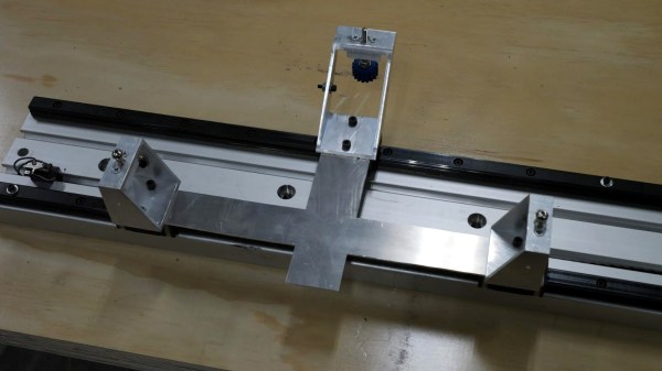
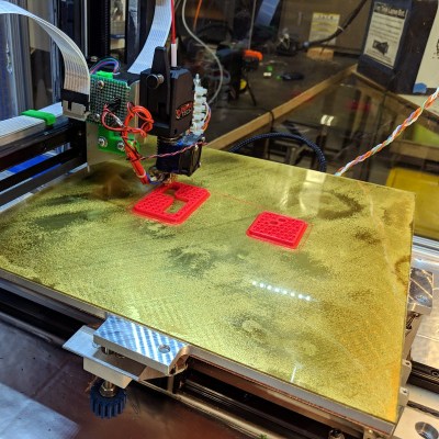
A Daylight-Readable Bar Graph Display In The 70s Wasn’t Cheap

The driver board with display attached; the row of lamps is visible on the right hand side.

LEDs weren’t always an easy solution to displays and indicators. The fine folks at [Industrial Alchemy] shared pictures of a device that shows what kind of effort and cost went into making a high brightness bar graph display in the 70s, back when LEDs were both expensive and not particularly bright. There are no strange materials or methods involved in making the display daylight-readable, but it’s a peek at how solving problems we take for granted today sometimes took a lot of expense and effort.

The display is a row of 28 small incandescent bulbs, mounted in a PCB and housed in a machined aluminum frame. Holes through which to view the bulbs are on both the top and front of the metal housing, which allows the unit to be mounted in different orientations. It was made as a swappable module, its 56 machined gold pins mate to sockets on the driver board. The driver board itself consists of 14 LM119 dual comparators, each of which controls two bulbs on the display.

An example of a Wamco minitron bar graph display. Each window contains an incandescent filament. [Source: industrialalchemy.org]
[Industrial Alchemy] believes that the display unit itself may have been a bit of a hack in its own way. Based on the pin spacing and dimensions of the driver board, they feel that it was probably designed to host a row of modular units known as the Wamco minitron bar graph display. An example is pictured here; they resembled DIP chips and could be stacked side-by-side to make a display of any length. Each window contained an incandescent filament in a reflective well, and each light could be individually controlled.

These minitron bar graph units could only be viewed from the top, and were apparently high in cost and low in availability. Getting around these limitations may have been worth creating this compatible unit despite the work involved.

Display technology has taken many different turns over the years, and you can see examples of many of them in one place in the Circus Clock, which tells the time with a different technology for each digit: a nixie, a numitron, a 7-segment thyratron tube, a VFD, an LED dot display, and a rear projection display.

What Good Are Counterfeit Parts? Believe It Or Not, Maybe A Refund

[Charles Ouweland] purchased some parts off Aliexpress and noticed that the Texas Instruments logo on some of his parts wasn’t the Texas Instruments logo at all, it was just some kind of abstract shape that vaguely resembled the logo. Suspicious and a little curious, he decided to take a closer look at the MCP1702 3.3v LDO regulators he ordered as well. Testing revealed that they were counterfeits with poor performance.

Left: counterfeit part. Right: genuine Microchip MCP1702-3302

Looking at the packages, there were some superficial differences in the markings of the counterfeit MCP1702 versus genuine parts from Microchip, but nothing obviously out of place. To conclusively test the devices, [Charles] referred to Microchip’s datasheet. It stated that the dropout voltage of the part should be measured by having the regulator supply the maximum rated 250 mA in short pulses to avoid any complications from the part heating up. After setting up an appropriate test circuit with a 555 timer to generate the pulses for low duty cycle activation, [Charles] discovered that the counterfeit parts did not meet Microchip specifications. While the suspect unit did output 3.3 V, the output oscillated badly after activation and the dropout voltage was 1.2 V, considerably higher than the typical dropout voltage of 525 mV for the part, and higher even than the maximum of 725 mV. His conclusion? The parts would be usable in the right conditions, but they were clearly fakes.

The usual recourse when one has received counterfeit parts is to dump them into the parts bin (or the trash) and perhaps strive to be less unlucky in the future, but [Charles] decided to submit a refund request and to his mild surprise, Aliexpress swiftly approved a refund for the substandard parts.

While a refund is appropriate, [Charles] seems to interpret the swift refund as a sort of admission of guilt on the part of the reseller. Is getting a refund for counterfeit parts a best-case outcome, evidence of wrongdoing, or simply an indication that low value refund requests get more easily approved? You be the judge of that, but if nothing else, [Charles] reminds us that fake parts may be useful for something perhaps unexpected: a refund.

Raspberry Pi PoE Redux

[Martin Rowan] was lucky enough to get his hands on the revised Power Over Ethernet (PoE) hat for the Raspberry Pi. Lucky for us, he wrote it up for our benefit, including inspection of the new hat, it’s circuit, and electrical testing to compare to the original hardware.

You may remember the original release of the PoE hat for the Raspberry Pi, as well as the subsequent recall due to over-current issues. In testing the revised board, [Martin] powered a test load off the USB ports, and pulled over an amp — The first iteration of the PoE hat would often trip the over-current protection at 300 milliamps.

This afternoon, the redesigned PoE board was officially released, and the post mortem of the problem documented in a blog post. It’s a lesson in the hidden complexity of hardware design, as well as a cautionary tale about the importance of thorough testing, even when the product is late and the pressure is on.

The PoE hat converts 48 volt power down to a 5 volt supply for the Pi using a flyback transformer. The problem was that this transformer setup doesn’t deliver clean steady 5 volt power, but instead provides power as a series of spikes. While these spikes were theoretically in spec for powering the Pi and usb devices, some Raspberry Pis were detecting those spikes as too much current pushed through the USB ports. The official solution essentially consists of better power filtering between the hat and the Pi, flattening that power draw.

We’re looking forward to getting our hands on this new and improved PoE Hat, and using it in many project to come.

The Negative Rail Explained

With the high availability of modular components and incredible wealth of information and tutorials online, it’s now easier than ever for hackers and makers to assemble complex electronic projects without getting bogged down with the theory behind it all. But the downside is that the modern electronic hobbyist often doesn’t have as deep an understanding of the low-level concepts that they would have if they had to build everything from scratch. This can be a problem when they try diagnosing and repairing faults, or when they start to branch out into reverse engineering.

Which makes “Building Blocks” by [David Christensen] a very compelling series. Every week he will be demonstrating a new circuit on his blog, complete with a plain English explanation of how and why it’s used. In this first installment of the series, he’s tackling a concept most of us have seen when poking around in more complex electronic devices, but maybe never really gave much thought to: the negative rail.

What exactly is the negative rail, anyway? It’s pretty easy to understand the positive rail in a circuit and its relation to ground; even multiple positive rails, such as in devices which use both 5 V and 3.3 V, are simple enough to wrap your head around. Unfortunately when something drops below that logical 0V reference, it isn’t quite as intuitive. But as [David] explains, the negative rail in a circuit is critical for dealing with bipolar signals, such as audio, which ride above and below the 0 V center point.

[David] goes over a few methods used to create the negative rail, from the classic center-tap transformer to using a buck-boost converter. But not content with just describing how these circuits work, he walks the reader through the creation of a charge pump circuit that you can drop into your next project if you find yourself in need of the elusive voltage. After explaining and diagramming it, he builds the circuit on a scrap piece of copper clad board and puts it through some benchmarks to prove it matches the theory he laid out.

If you’re in the mood for more negative talk, check out the battle our very own [Steven Dufresne] had with voltages of varying polarity when building his BB-8 robot.

The Dual In-Line Package And How It Got That Way

For most of human history, our inventions and innovations have been at a scale that’s literally easy to grasp. From the largest cathedral to the finest pocket watch, everything that went into our constructions has been something we could see with our own eyes and manipulate with our hands. But in the middle of the 20th century, we started making really, really small stuff: semiconductors. For the first time, we were able to create mechanisms too small to be seen with the naked eye, and too fine to handle with our comparatively huge hands. We needed a way to scale these devices up somewhat to make them useful parts. In short, they needed to be packaged.

We know that the first commercially important integrated circuits were packaged in the now-familiar dual in-line package (DIP), the little black plastic millipedes that would crawl across circuit boards for the next 50 years. As useful and versatile as the DIP was, and for as successful as the package became, its design was anything but obvious. Let’s take a look at the dual in-line package and how it got that way.

Continue reading “The Dual In-Line Package And How It Got That Way”

Steady Hand Repurposes Cheap SSD Modules

For hackers, cheap (and arguably disposable) consumer hardware makes for a ready supply of free or low-cost components. When you can walk into a big box store and pick up a new low-end laptop for $150, how many are going to spend the money to repair or upgrade the one they have now? So the old ones go to the bin, or get sold online for parts. From an ecological standpoint our disposable society is terrible, but at least we get some tech bargains out of the deal.

Case in point, the dirt cheap 32 GB eMMC SSDs [Jason Gin] recently scored. Used by Hewlett Packard on their line of budget laptops, he was able to snap up some of these custom drives for only $12 each. Only problem was, since they were designed for a very specific market and use case, they aren’t exactly the kind of thing you can just slap in your computer’s drive bay. He had to do some reverse engineering to figure out how to talk to them, and then some impressive fine-pitch soldering to get them plugged in, but in the end he got some very handy drives for an exceptionally low price.

[Jason] starts by figuring out the drive’s pinout using the cornerstone of the hacker’s electronic toolkit: the multimeter. By putting one lead on an obvious ground point such as the PCB’s screw holes, you can work through the pins on the connector and make some educated guesses as to what’s what. Ground pins will read as a short, but the meter should read power and data pins as a forward-biased diode. With a rough idea of the pin’s identities and some luck, he was able to figure out that it was basically a standard SATA connection in a different form factor.

To actually hook it up to his computer, he pulled the PCB off of a dead SATA hard drive, cut it down to size, and was able to use fine magnet wire to attach the conductors in the drive’s ribbon cable to the appropriate pads. He sealed everything up with a healthy dose of hot glue to make sure it didn’t pull loose, and then ran some drive diagnostics on his cobbled together SSD to make sure it was behaving properly. [Jason] reports the drive isn’t exactly a speed demon, but given the low cost and decent performance he still thinks it’s worth the work to use them for testing out different operating systems and the like.

[Jason] seems to have something of an obsession with eMMC hacking. Last time we heard from him, he was bringing a cheap Windows tablet back from the dead by replacing its shot eMMC chip.

Teardown Of A (Relatively) Cheap Thermal Camera

The cost of tools and test equipment has largely been on the downward trend for years, making it now more affordable than ever to get into the hacking and making scene. This is particularly visible with something like the venerable oscilloscope: a piece of equipment that was near unobtainium for the home hacker a decade ago, you can now get digital pocket scope for as little as $20 USD. But there are still pieces of gear which haven’t quite hit the sort of prices we’d like to see.

A perfect example are thermal imaging cameras. The cheap ones are usually so low resolution they might as well just be thermometers, but the higher resolution ones can cost thousands. [Rob Scott] recently wrote in to tell us about a very promising middle ground, the HTI HT-A1. But he didn’t just point it out to us, he also tore it down and laid its internal’s bare for our entertainment. Now that’s our kind of introduction.

[Rob] walks us through the disassembly of the device, which is made unnecessarily difficult due to the fact that half the screws are hidden under a glued on screen bezel. That means a heat gun, a thin tool, and patience are in order if you want to get inside the device. It’s bad enough they use these kinds of construction techniques on modern smartphones, but at least they’re so thin that we can understand the reasoning. Why this chunky thing needs to resort to such measures is beyond us.

Eventually he cracks the HT-A1 open and is greeted with a single double-sided PCB. The top side is pretty much bare except for the buttons and the LCD display, and the flip side is largely just a breakout for a quad-core Allwinner A33 daughterboard. [Rob] theorizes this is to keep costs down by allowing reuse of the modular A33 board on other devices. Given the A33’s use in so many cheap tablets, it’s also possible HTI simply purchased these daughterboards as a drop-in component and designed their own board around it.

There’s not much else inside the HT-A1 beyond the rechargeable battery pack and thermal camera, both attached to the device’s rear panel. [Rob] noticed that the date on the thermal camera PCB is a full two years older than the date on the main PCB, leading one to wonder if HTI might have gotten a good deal on a bunch of these slightly outdated sensors and spun up a whole device around them.

The HT-A1 is high enough resolution that you can actually pick out individual components on a PCB, and at $400 USD is approaching a reasonable price point for the individual hacker. Which is not to say it’s cheap, but at least you get a useful tool for your money. We wouldn’t suggest you buy this device on a whim, but if you do a lot of diagnostic work, it might pay for itself after a couple repairs.

If that’s still a little too rich for your blood, we’ve covered a handful of DIY options which might better fit your budget.

Continue reading “Teardown Of A (Relatively) Cheap Thermal Camera”