How A Quadriplegic Patient Was Able To Eat By Himself Again Using Artificial Limbs

Thirty years ago, [Robert “Buz” Chmielewski] suffered a surfing accident as a teenager. This left him as a quadriplegic due to a C6 spinal cord injury. After becoming a participant in a brain-computer interface study at Johns Hopkins, he was recently able to feed himself through the use of prosthetic arms. The most remarkable thing about these prosthetic arms is primarily the neural link with [Buz’s] brain, which allows him to not only control the artificial arms, but also feel what they are touching, due to a closed-loop system which transfers limb sensory input to the patient’s brain.

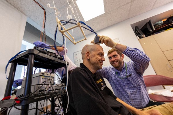
The prosthetic limb in question is the Modular Prosthetic Limb (MPL) from Johns Hopkins Applied Physics Laboratory (APL). The Johns Hopkins Medicine Brain-Computer Interface study began a year ago, when [Buz] had six microelectrode arrays (MEA) implanted into his brain: half in the motor cortex and half in the sensory cortex. During the following months, the study focused on using the signals from the first set of arrays to control actuators, such as the MPL. The second set of arrays was used to study how the sensory cortex had to be stimulated to allow a patient to feel the artificial limb much as one feels a biological limb.

What makes this study so interesting is not only the closed-loop approach which provides the patient with feedback on the position and pressure on the prosthetic, but also that it involves both hemispheres of the brain. As a result, after only a year of the study, [Buz] was able to use two of the MPLs simultaneously to feed himself, which is a delicate and complicated tasks.

In the video embedded after the break one can see a comparison of [Buz] at the beginning of the study and today, as he manages to handle cutlery and eat cake, without assistance.

Continue reading “How A Quadriplegic Patient Was Able To Eat By Himself Again Using Artificial Limbs”

LEDs-On-Chips Will Give Us Lower Cost Optoelectronics

The LED is one of those fundamental building block components in electronics, something that’s been in the parts bin for decades. But while a simple LED costs pennies, that WS2812 or other fancy device is a bit expensive because internally it’s a hybrid of a silicon controller chip and several LEDs made from other semiconductor elements. Incorporating an LED on the same chip as its controller has remained something of a Holy Grail, and now an MIT team appear to have cracked it by demonstrating a CMOS device that integrates a practical silicon LED. It may not yet be ready for market but it already displays some interesting properties such as a very fast switching speed. Perhaps more importantly, further integration of what have traditionally been discrete components would have a huge impact on reducing manufacturing costs.

Anyone who has read up on the early history of LEDs will know that the path from the early-20th-century discoveries of semiconductor luminescence through the early commercial devices of the 1960s and up to the bright multi-hued devices of today has been a long one with many stages of the technology reaching the market. Thus these early experimental silicon LEDs produce light in the infrared spectrum often useful in producing sensors. Whether we’ll see an all-silicon Neopixel any time soon remains to be seen, but we can imagine that some sensors using LEDs could be incorporated on the same die as a microcontroller. It seems there’s plenty of potential for this invention.

This research was presented earlier this month at the IEDM Conference in a talk entitled Low Voltage, High Brightness CMOS LEDs. We were not able to find a published paper, we’d love read deeper so let us know in the comments below if you have info on when this will become available. In the meantime, anyone with any interest in LED technology should read about Oleg Losev, the inventor of the first practical LEDs.

Magnetocuring: Curing Epoxy With A Magnetic Field

Who doesn’t love epoxy? Epoxy resins, also known as polyepoxides, are an essential adhesive in many applications, both industrially and at smaller scales. Many polyepoxides however require the application of heat (around 150 °C for most types) in order to cure (harden), which can be complicated when the resin is applied to or inside layers of temperature sensitive materials. Now researchers at Nanyang Technological University (NTU) in Singapore have found a way to heat up resins using an alternating magnetic field (PDF), so-called magnetocuring.

As detailed in the research article by R. Chaudhary et al., they used commercially available epoxy resin and added nano particles of a MnxZn1-xFe2O4 alloy. This mixture was exposed to an alternating magnetic field to induce currents in the nano particles and subsequently produce heat that served to raise the temperature of the surrounding resin to about 160 °C in five minutes, allowing the resin to cure. There is no risk of overheating, as the nano particles are engineered to reach their Curie temperature, at which point the magnetic field no longer affects them. The exact Curie temperature was tweaked by changing the amount of manganese and zinc in the alloy.

After trying out a number of different alloy formulations, they settled on Mn0.7Zn0.3Fe2O4 as the optimal formulation at which no resin scorching occurred. As with all research it’s hard to tell when (and if) it will make it into commercial applications, but if this type of technology works out we could soon be gluing parts together using epoxy resin and an EM field instead of fumbling with the joys of two-component epoxy.

(Thanks, Qes)

Seeking Enlightenment: The Quest To Restore Vision In Humans

Visual impairment has been a major issue for humankind for its entire history, but has become more pressing with society’s evolution into a world which revolves around visual acuity. Whether it’s about navigating a busy city or interacting with the countless screens that fill modern life, coping with reduced or no vision is a challenge. For countless individuals, the use of braille and accessibility technology such as screen readers is essential to interact with the world around them.

For refractive visual impairment we currently have a range of solutions, from glasses and contact lenses to more permanent options like LASIK and similar which seek to fix the refractive problem by burning away part of the cornea. When the eye’s lens itself has been damaged (e.g. with cataracts), it can be replaced with an artificial lens.

But what if the retina or optic nerve has been damaged in some way? For individuals with such (nerve) damage there has for decades been the tempting and seemingly futuristic concept to restore vision, whether through biological or technological means. Quite recently, there have been a number of studies which explore both approaches, with promising results.

Continue reading “Seeking Enlightenment: The Quest To Restore Vision In Humans”

Twenty Seconds At 100 Megakelvins

The Korea Superconducting Tokamak Advanced Research (KSTAR) magnetic fusion reactor claimed a new record last month — containing hydrogen plasma at 100 megakelvins for 20 seconds. For reference, the core temperature of the Earth’s Sun is a mere 15 megakelvins, although to be fair, it has been in operation quite a bit longer than 20 seconds.

South Korea is a member of the International Thermonuclear Experimental Reactor (ITER) team, a worldwide project researching the science and engineering of nuclear fusion. One of their contributions to the effort is the KSTAR facility, located in the city of Daejeon in the middle of the country (about 150 km south of Seoul).

It is a tokamak-style fusion research reactor using superconducting magnets to generate a magnetic flux density of 3.5 teslas and a plasma current of 2 megaamperes. These conditions are used to confine and maintain the plasma in what’s called the high-confinement mode, the conditions currently favored for fusion reactor designs. Since it went into operation in 2008, it has been creating increasingly longer and hotter “pulses” of plasma.

For all the impressive numbers, the toroidal reactor itself is not that huge. Its major diameter is only 3.6 meters with a minor diameter of 1 meter. What makes the facility so large is all the supporting equipment. Check out the video below — we really like the techniques they use in this virtual tour to highlight key components of the installation.

Continue reading “Twenty Seconds At 100 Megakelvins”

Hello, Holograms

Holograms are tricky to describe because science-fiction gives the name to any three-dimensional image. The science-fact versions are not as flashy, but they are still darn cool. Legitimate holograms are images stored on a photographic medium, and they retain a picture of the subject from certain angles. In other words, when [Justin Atkin] makes a hologram of a model building, (video, embedded below) you can see the east side of the belfry, but when you reorient, you see the west side, or the roof if you point down. Holography is different from stereoscopy, which shows you a 3D image using two cameras. With a stereoscopic image, you cannot tilt it and see a new part of the subject, so there is a niche for each method.

There are a couple of different methods for making a hologram at home. First, you probably want a DIY hologram kit since it will come with the exposure plate and a known-good light source. Far be it for us to tell you you can’t buy plates and a laser pointer to take the path less traveled. Next, you need something that will not move, so we’re afraid you cannot immortalize your rambunctious kitty. The last necessity is a stable platform since you will perform a long-exposure shot, and even breathing on the setup can ruin the image. Different colors come from the coherent light source, so getting the “Rainbow Holograms” advertised in the video is a matter of mixing lights. Since you can buy red, green, and blue laser pointers for a pittance, you can do color remixes to your content.

Another type of hologram appears on things like trading cards as those wildly off-color (chromatic, not distasteful) images of super-heroes or abstract shapes. They’re a different variety, which can be printed en-masse, unlike the one-off [Justin] shows us how to make.

If you’re yearning for volumetric displays, we are happy to point you to this beauty capable of showing a jaw-dropping 3D model or this full-color blocky duck.

Continue reading “Hello, Holograms”

The Mouth-Watering World Of NIST Standard Foods

The National Institute Of Standards and Technology was founded on March 3, 1901 as the National Bureau of Standards, taking on its current moniker in 1988. The organisation is charged by the government with ensuring the uniformity of weights and measures across the United States, and generally helping out industry, academia and other users wherever some kind of overarching standard is required.

One of the primary jobs of NIST is the production and sale of Standard Reference Materials, or SRMs. These cover a huge variety of applications, from steel samples to concrete and geological materials like clay. However, there are also edible SRMS, too. Yes, you can purchase yourself a jar of NIST Standard Peanut Butter, though you might find the price uncompetitive with the varieties at your local supermarket. Let’s dive into why these “standard” foods exist, and see what’s available from the shelves of our favourite national standards institute. Continue reading “The Mouth-Watering World Of NIST Standard Foods”