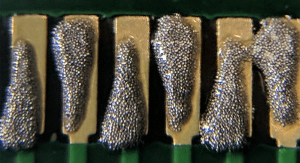
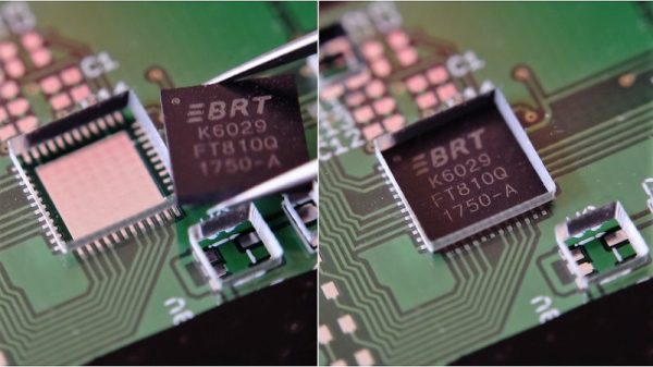
If there’s one thing that will bring down the yield of your PCB assembly, it’s your solder paste. Put too much on, and you’ll get bridged leads. If you don’t put enough on, that pad might not make good contact. [ScalarElectric] has an amazing trick that’s sure to astonish and astound. Just use wedges and you’ll get better yield with fine-pitched components.
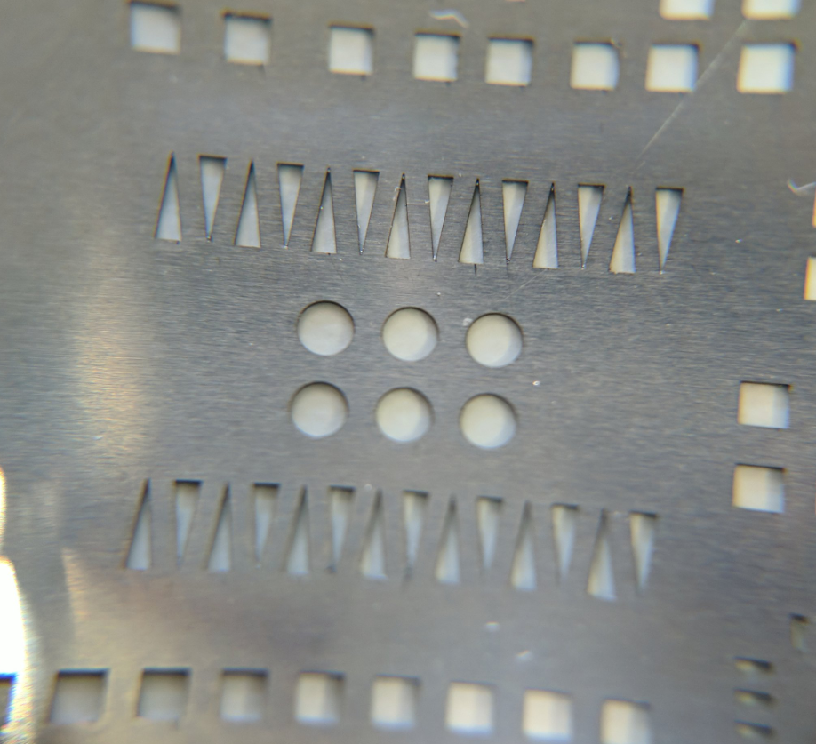
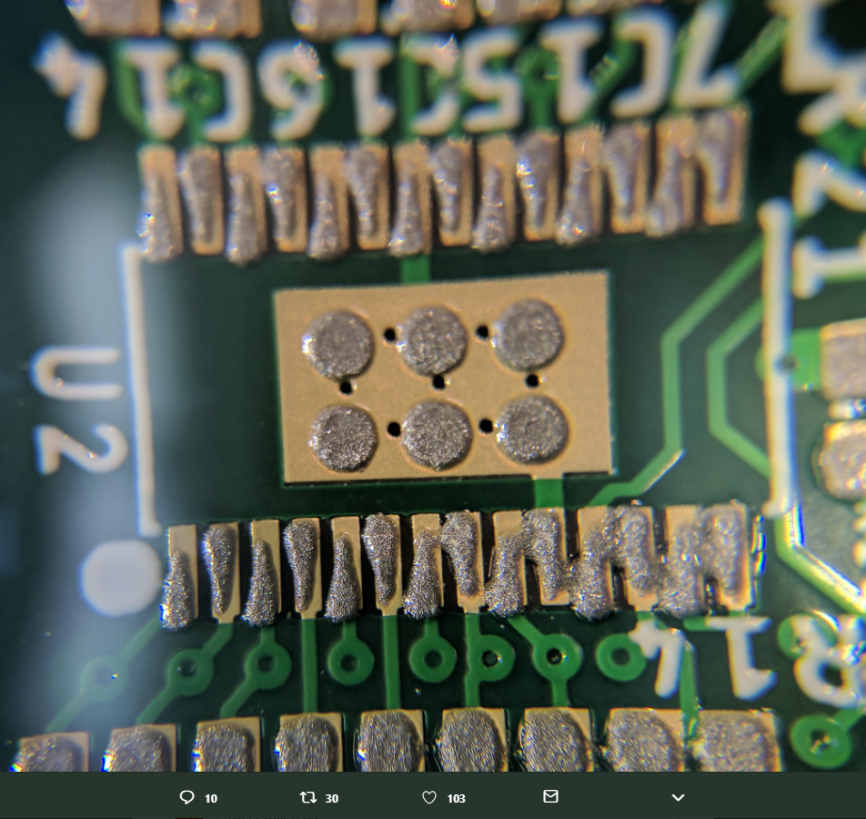
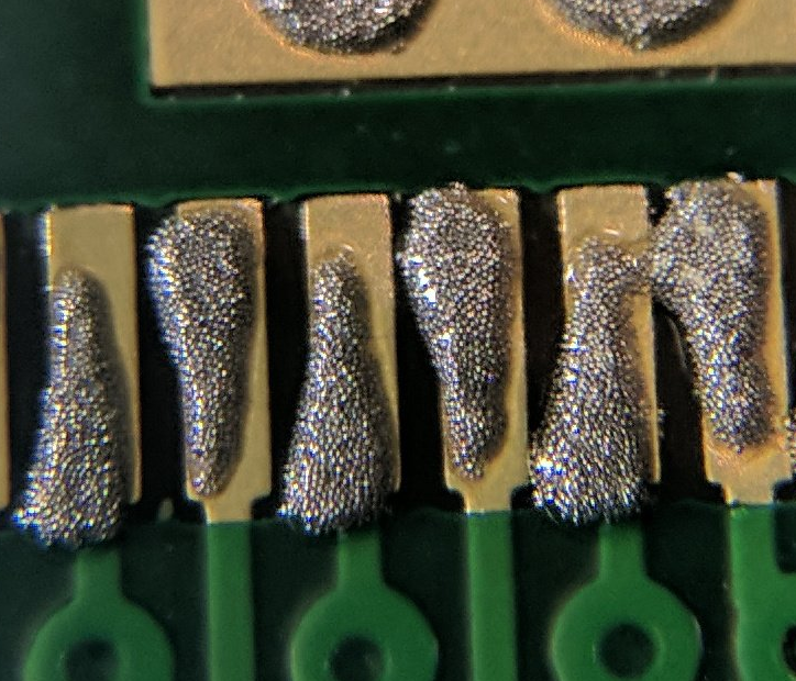
The trick here is to define the cream/solder paste layer of each package as a wedge on each pad instead of the usual rectangle. This gives a few benefits, the largest being the increased gap between paste shapes. You’re also getting a reduction in the total amount of paste applied, and a subsequent improvement in yield. (Reportedly, we’d love to see some data on this.)
PCB design tools usually have a way to alter the size of the cream/solder paste layer of a design, and indeed one option is to simply shrink the size of the paste layer elements. The trick to the wedges is increasing the total distance between solderpaste blobs while keeping the total amount of solderpaste high. This technique can be used down to 0.5mm pitch parts, and everything works like a charm.
While this is a little outside of our wheelhouse here at Hackaday — it is, after all, a novel use of existing tools that is mostly applicable to electronic design and production. [Ed Note: Sarcasm.] You can check out a few pics of this technique in the slideshow below. If you test this technique out, be sure to let us know how it went!


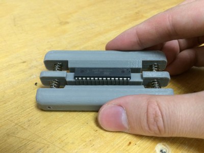 Fresh from the factory Dual Inline Package (DIP) chips come with their legs splayed every so slightly apart — enough to not fit into the carefully designed footprints on a circuit board. You may be used to imprecisely bending them by hand on the surface of the bench. [Marco] is more refined and shows off a neat little spring loaded tool that just takes a couple of squeezes to neatly bend both sides of the DIP, leaving every leg the perfect angle. Shown here is
 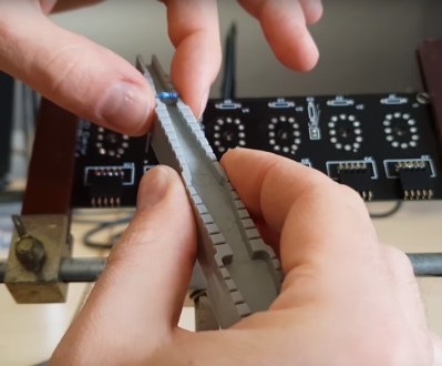 Another tool which caught our eye is the one he uses for bending the metal film resistor leads: the “Biegelehre” or lead bending tool. You can see that [Marco’s] tool has an angled trench to account for different resistor body widths, with stepped edges for standard PCB footprint spacing. We bet you frequently use the same resistor bodies so 3D printing is made easier by