The Apple II was the popular darling that truly kicked off the ascention of the company that would later bring you darlings such as the iMac, iPod, and iPhone. The brainchild of the legendary Steve Wozniak, it was a low-cost home computer that made use of some interesting compromises to create video output with the bare minimum components. This can make it difficult if you want to output full-bitmap graphics on the Apple II – but it is certainly possible.
[cybernesto] set about completing this task, and released VBMP on GitHub. Programmed in assembly, it builds upon the work of democoder Arnaud Cocquière to display bitmap images on the vintage 6502-powered machine. Capable of displaying monochrome images in 560 x 192 or sixteen colors in 140 x 192, it loads slowly but does get the job done.
We’ve seen similar development underway elsewhere, too – on this vintage satellite tracker project. [Keplermatic] reports that their code runs at a similar speed to the VBMP loader, despite doing several things differently. It’s also available over at GitHub, for your reading pleasure.
If you’re looking to achieve something similar with your vintage hardware, it’s worth a look. Having the source available makes integrating it into further projects a snap. Learning to program these older machines can be challenging, but that’s half the fun – and when you build something awesome, be sure to drop it on the tips line.
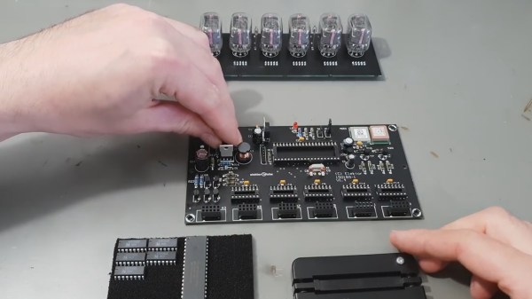
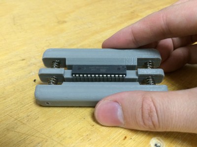 Fresh from the factory Dual Inline Package (DIP) chips come with their legs splayed every so slightly apart — enough to not fit into the carefully designed footprints on a circuit board. You may be used to imprecisely bending them by hand on the surface of the bench. [Marco] is more refined and shows off a neat little spring loaded tool that just takes a couple of squeezes to neatly bend both sides of the DIP, leaving every leg the perfect angle. Shown here is
 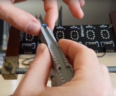 Another tool which caught our eye is the one he uses for bending the metal film resistor leads: the “Biegelehre” or lead bending tool. You can see that [Marco’s] tool has an angled trench to account for different resistor body widths, with stepped edges for standard PCB footprint spacing. We bet you frequently use the same resistor bodies so 3D printing is made easier by