Is twenty times the copper twenty times as much fun to work with? Ask [limpkin] and follow along as he fabricates a DC/DC block for a Formula E race car on 20-oz copper PCBs.
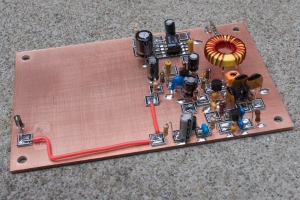
The typical boards you order from OSH Park and the like usually come with 1-ounce copper – that’s one ounce of copper cladding per square foot of board. For those averse to Imperial units, that’s a copper layer 34 micrometers thick. [limpkin]’s Formula E control board needs to carry a lot of current, so he specified 700-micrometer thick cladding, or 20-oz per square foot. The board pictured cost $2250, so you’d figure soldering on the components would be an exotic process, but aside from preheating the board, [limpkin] took it in stride. Check out the image gallery of the session and you’ll see nothing but a couple of regular high-wattage soldering irons, with dirty tips to boot.
It’s pretty neat comparing what’s needed for power electronics versus the normal small signal stuff we usually see. We’d recommend looking at [Brian Benchoff]’s “Creating a PCB in Everything” series for design tips, but we’re not sure traditional tools will work for boards like these. And just for fun, check out the Formula E highlights video below the break to see what this build is part of.
Continue reading “Massive 20-oz. Copper PCB Enables Electric Racing”