Not every computer is a performance gaming rig. Some of us need cheap laptops and tablets for simple Internet browsing or word processing, and we don’t need to shell out thousands of dollars just for that. With a cheaper price tag comes cheaper hardware, though, such as the eMMC standard which allows flash memory to be used in a more cost-advantageous way than SSDs. For a look at some the finer points of eMMC chips, we’ll turn to [Jason]’s latest project.
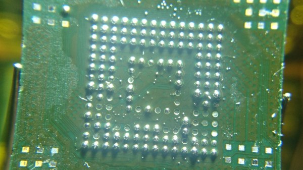
[Jason] had a few damaged eMMC storage chips and wanted to try to repair them. The most common failure mode for his chips is “cratering” which is a type of damage to the solder that holds them to their PCBs. With so many pins in such a small area, and with small pins themselves, often traditional soldering methods won’t work. The method that [Jason] found which works the best is using 0.15 mm thick glass strips to aid in the reflow process and get the solder to stick back to the chip again.
Doing work like this can get frustrating due to the small sizes involved and the amount of heat needed to get the solder to behave properly. For example, upgrading the memory chip in an iPhone took an expert solderer numerous tries with practice hardware to finally get enough courage to attempt this soldering on his own phone. With enough practice, the right tools, and a steady hand, though, these types of projects are definitely within reach.
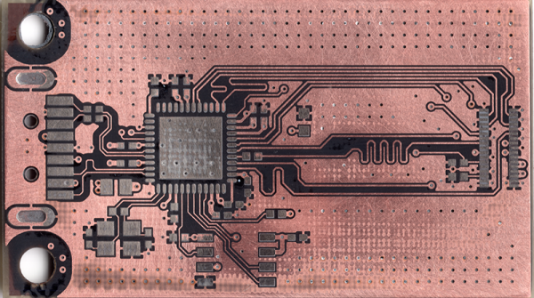
Every once in a while, and more so now than before, you’ll find a really neat chip with zero documentation. In [David]’s case, it’s a really cool USB 3.0 eMMC/ SD MMC controller. Use this chip, attach a USB port on one end, and some memory on the other, and you have a complete bridge. There are drivers, too. There are products shipping with this chip. The problem is, there is no data sheet. Wanting to use this chip, [David] turned to sandpaper to figure out the pinout of this chip.
The best example of a product that came with this chip is a simple board from the hardkernel store that happily came with fairly high resolution product photos. While waiting for these boards to be delivered, [David] traced the top layer of copper. This was enough to get an idea of what was going on, but the real work started when the boards arrived. These were placed in a flatbed scanner and carefully photographed.
The next step was to desolder all the parts, taking care to measure and catalog each component. Then, it’s off to sanding with 200 and 600 grit wet sandpaper. Slowly, the soldermask is removed and the top copper layer appears. After that, it’s just a matter of sanding and scanning, stacking all the layers together with your image processing software of choice.
There are a few caveats to hand-sanding a PCB to reverse-engineer the copper layers. First, it makes a mess. This is wet/dry sandpaper, though, and you can and should sand with water. Secondly, even pressure should be applied. We’re not sure if [David] was holding the sandpaper or not, but the best technique is to actually hold the board itself.
Despite a few problems, [David] did get the pictures of each copper layer. After assembling these images, he could make an Eagle part for an eMMC reader for his Nintendo Switch.
We’ve probably all got at least one old cell phone lurking somewhere around our bench. In most cases they’ll still work, but their batteries may be exhausted and their OS could be an ancient version. But sometimes there will be a phone that just died. One minute the flagship model, the next a useless slab of plastic and glass with the added annoyance of those priceless photos of Aunty May’s 80th forever locked in its memory.
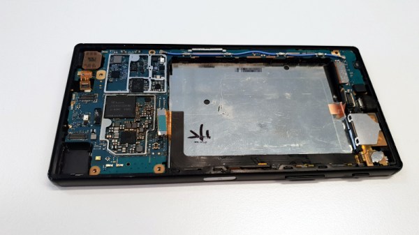
[Andras Kabai] had just such a device land on his desk, a high-end Sony whose screen had gone blank. Others had tried, he was the last hope for the data it contained. He zoomed in on the eMMC chip on its motherboard, desoldered it and hooked it up via a specialist eMMC reader to recover those files. That was a very simple description of a far more involved process that he sets out in his post about it, a post that is fascinating reading and serves as a handy primer for any reader who might like to try it for themselves. We learn about the MMC interface and how simple it can be in its serial form, how with some fine soldering you can use a cheap USB reader, and that eMMC chips have a pinout conforming to a JEDEC standard.
Finally we see the software side as he takes the various SQLite databases and extracts the data for the user. It shows, all is not necessarily lost, however dead a phone may be.
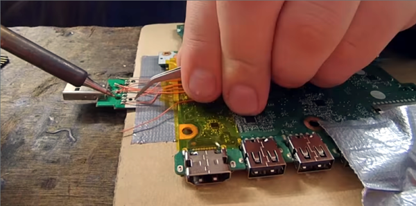
What happens when you drop your laptop in the pool? Well, yes, you buy a new laptop. But what about your data. You do have backups, right? No, of course, you don’t. But if you can solder like [TheRasteri] you could wire into the flash memory on the motherboard and read it one last time. You can see the whole exploit in the video below.
There’s really three tasks involved. First is finding the schematic and board layout for motherboard. Apparently, these aren’t usually available from the manufacturer but can be acquired in some of the seedier parts of the Internet for a small fee. Once you have the layout, you have to arrange to solder wires to the parts of the flash memory you need to access.
[Jason Gin] recently wrote in to tell us about his adventures replacing the eMMC storage chip on a cheap Windows tablet, and we have to say, it’s an impressive amount of work for a device which apparently only cost him $15. Surely much better pieces of hardware have been tossed in the trash for less serious failures than what ailed his DigiLand DL801W tablet. We’d love to see the lengths this guy would go to restore something a bit higher up the food chain.
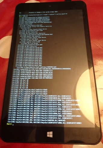
As any good hacker knows, you can’t fix the problem until you understand it. So the first step [Jason] took was to conduct some troubleshooting. The tablet would only boot to the EFI shell, which didn’t do him much good since there was no on-screen keyboard to interact with it. But he had the idea of trying to connect a USB keyboard via an OTG adapter, and sure enough that got him in. Once he was able to enter commands into the EFI shell, he attempted to read from a few different sectors of the eMMC drive, only to get the same nonsense repeating data. So far, not looking good.
But before he fully committed to replacing the eMMC drive, he wanted a second opinion. Using the same USB OTG adapter, he was able to boot the tablet into a Windows 10 environment, and from there got access to some drive diagnostic tools. The software reported that not only was the drive reporting to be half the appropriate size, but that writing to the chip was impossible.
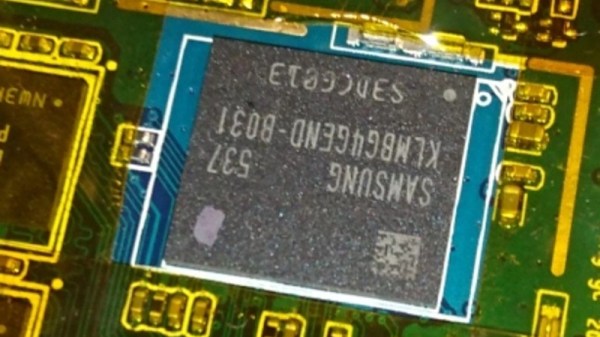
With the fate of the tablet’s Foresee NCEMBS99-16G eMMC chip now confirmed, [Jason] decided it was time to operate. After pulling the tablet apart and masking off the PCB with Kapton tape to protect it from the heat, he slowly went in with his hot air rework station to remove the failed chip. But rather than put another low-end chip in its place, he used this opportunity to replace it with a Samsung KLMBG4GEND-B031. Not only does this chip have twice the capacity of the original, it should be noticeably faster.
With the new Samsung eMMC chip installed, [Jason] put the tablet back together and was able to successfully install Windows 10 onto it. Another piece of tech saved from the big landfill in the sky.
There’s a natural order to the world of game console hacking: every time a manufacturer releases a new game console they work in security measures that prevent the end user from running anything but commercially released games, and in turn every hacker worth his or her salt tries to break through. The end goal, despite what the manufacturers may have you believe, is not to run “bootleg” games, but rather to enable what is colloquially referred to as “homebrew”. That is to say, enabling the novel concept of actually running software of your choice on the hardware you paid for.
At 34C3, noted console hackers [Plutoo], [Derrek], and [Naehrwert] have demonstrated unsigned code running on Nintendo’s latest and greatest and while they are keeping the actual exploit to themselves for now, they’ve promised that a platform for launching homebrew is coming shortly for those who are on firmware version 3.0.0. From the sound of it, after 9 months on the market, Switch owners will finally have complete access to the hardware they purchased.
The key to running the team’s own code was through a WebKit exploit that was already months old by the time the Switch was released. Loading up an arbitrary webpage was the tricky part, as the Switch generally uses its web browser for accessing official sources (like the online game store). But hidden away in the help menus of Tetris, the developers helpfully put a link to their website which the Switch will dutifully open if you select it. From there it’s just a matter of network redirection to get the Switch loading a webpage from your computer rather than the Internet.
It’s easier to ask for forgiveness than permission.
But as the more security-minded of our readers may have guessed already, that just gets you into the browser’s sandbox. The team now had to figure out a way to break out and get full control of the hardware. Through a series of clever hacks the team was able to learn more about the Switch’s internal layout and operating system, slowly working their way up the ladder.
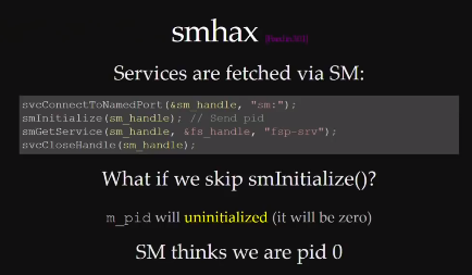
A particularly interesting hack was used to get around a part of the Switch’s OS that is designed to check which services code is allowed to access. It turns out that if code doesn’t provide this function with its own process ID (PID), the system defaults to PID 0 because the variable is not initialized. In other words, if you don’t ask the operating system which functions you have access to, you will get access to them all. This is a classic programming mistake, and a developer at Nintendo HQ is likely getting a very stern talking to right about now.
But not everything was so easy. When trying to get access to the boot loader, the team sniffed the eMMC bus and timed the commands to determine when it was checking the encryption keys. They were then able to assemble a “glitcher” which fiddled with the CPU’s power using FPGA controlled MOFSETs during this critical time in an attempt to confuse the system.
The rabbit hole is pretty deep on this one, so we’d recommend you set aside an hour to watch the entire presentation to see the long road it took to go from a browser bug to running their first complete demo. It’s as much a testament to the skill of [Plutoo], [Derrek], and [Naehrwert] as it is the lengths at which Nintendo went to keep people out.
In unlocking the extra performance, he takes readers through a primer on the device tree, and is happy to report that his transfer rate has increased from 26 to 36 MB/s, a tidy return on his work.
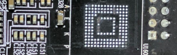
However, the story doesn’t end there. The 8GB Samsung eMMC chip wasn’t quite as roomy as he’d have liked, so it was time to replace it with a 32GB version. Even with careful desoldering, he managed to lift a few pads, though very fortunately they were ones that were either NC or power rails that were duplicated elsewhere. Some tricky reflowing of what is quite a formidable BGA package to do by hand, and he was rewarded with a working board featuring higher flash capacity. We salute him for taking it on, we probably wouldn’t have had the courage.