Munged Ferris Bueller quotes aside, Conway’s Game of Life is the classic cellular automata that we all reach for. The usual approach is to just iterate over every cell in the grid, computing the next state into a new grid buffer. [K155LA3] set out to turn that on its head by implementing Game Of Life in the hardware of an FPGA.
[K155LA3]’s version uses Chisel, a new HDL from the Berkley and RISCV communities. Under the hood, Chisel is Scala with some custom libraries that know how to map Scala concepts onto hardware. In broad strokes, Verilog and VHDL are focused on expressing hardware and then added abstraction on top of that over the year. Chisel and other newer HDL languages focus on expressing high-level general-purpose elements that get mapped onto hardware. FPGAs already map complex circuits and hardware onto LUTs and other slices, so what’s another layer of abstraction?
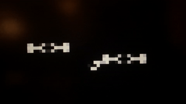
The FPGA chosen for this project is a Digilent Arty A7 with a VGA Pmod to turn the RGB444 into analog signals to actually display. What’s impressive about [K155LA3]’s implementation is just how fast it is. Even running at 60 frames per second it’s almost as fast as the monitor can handle. Of course, most computers lying around you could simulate a 60 x4 8 grid at 60 fps. Next, instead of connecting the grid logic to the 60 Hz VGA clock, he connects it to the 100 MHz board external oscillator. Now each pixel in each frame displayed contains over a million generations.
Unfortunately, even this small grid of 60×48 takes up 90% of the LUTs on the Artix-7. In the future, we’d love to see an even larger FPGA hardware implementation capable of handling grids that could hold whole computers in them. And naturally, this isn’t the first FPGA version of the Game Of Life here at Hackaday.