A 1981 Centaur pinball table rebuilt into a coffee table.

Clear Off The Coffee Table, It’s Pinball Time

Like many of us, [BuildXYZ] has always wanted to own a pinball machine, but doesn’t have the space to justify buying such a big and heavy toy. But where there’s a will, there’s a way. [BuildXYZ] figured that if they could build a pinball machine into a coffee table form factor, they’d be at least halfway to justification.

[BuildXYZ] didn’t choose just any pin. After doing a bunch of research, they settled on 1981’s Bally Centaur because it’s an early solid-state machine, and it’s one of the best. It has no secondary playfield levels to deal with, making it much easier to do this project.

Where do we even start to describe this beautiful labor of love? There are too many details to list, but know that it seems to be equal amounts of restoration work and custom work that brought this table together. The build video after the break is definitely worth your time, and you’ll gain a much better appreciation of the amount of time that went into this, from the custom score decoder chip built on an FPGA to the 3D printed replacement drop targets and new acrylic bits to replace the yellowing ones from the playfield.

Continue reading “Clear Off The Coffee Table, It’s Pinball Time”

6502 Goes FPGA (Again)

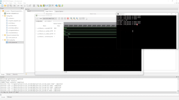
While there has been no shortage of FPGA-based recreations of classic processors, we always enjoy seeing a new approach. Last month [Some Assembly Required] took on the challenge to recreate a classic computer from the ground up and started with a 6502 implementation in Verilog. You can see in the second video below that he’s made good progress and there are apparently more videos to come.

The ROL instruction is the subject of the second video. We liked the approach of looking at what the instruction does and how many cycles it takes on different variants It is always good to make sure you know exactly what you are trying to accomplish before you get started.

Continue reading “6502 Goes FPGA (Again)”

X-ray image of a camera lens

Observing A Plant’s Vascular System With X-Ray Video

[Ben Krasnow] has a knack for showing us what’s inside of things while they’re moving. This week’s Applied Science experiment has him making time-lapse X-ray videos of things. This plant’s vascular system is just one of a few examples, the others being a dial clock and the zoom lens on a DSLR.

X-ray of plantThe trick here is having an X-ray sensing panel that can be reused. It takes around five seconds of exposure to grab each 40×40 cm frame which are then assembled back into video.

Now watching mechanisms move is cool — [Ben’s] video back in 2015 to show what a phonograph needle in the groove of a vinyl record looks like under a scanning electron microscope is still one for the coolest “camera tricks” we’ve ever seen pulled off. But watching the vascular system of a plant function is the recipe for one of those ah-ha educational moments, so we hope that 7th-grade biology teachers everywhere will find their way to this video.

The apparatus is described in great detail, but regular Hackaday readers will most likely want to focus in on the teardown of the X-ray panel, which [Ben] describes as a giant digital camera sensor tuned for receiving the X-rays. The source is a 50 kV 1 mA tube that he compares to what is used at the dental office. (Obviously this requires forethought to ensure his automated time-lapse setup will fail safe with the X-ray tube.) A Cyclone III FPGA drives the panel, communicating with the sensor array via two Ethernet interfaces.

A friend sent a the broken panel to [Ben] and he was able to easily repair a MOSFET that got knocked out of place. [biluni] shows up in the comments of this video, sharing his recollection from working in the industry 15 years ago that a panel like this would have cost $150k! But considering the stellar resolution, and repeatable use, it sure as heck beats the old film process.

Continue reading “Observing A Plant’s Vascular System With X-Ray Video”

Using VHDL To Generate Discrete Logic PCB Designs

VHDL and Verilog are hardware description languages, used to describe and define logic circuits. They’re typically used to design ASICs and to program FPGAs, essentially using software to define hardware. However, [Tim] has done something altogether quite creative, creating tools to take VHDL and Verilog and spit out PCB designs for discrete logic. 

Yes, you read that correctly. The basic idea is to take VHDL source code, and then make a PCB layout that implements the desired logic using resistor-transistor logic. From there, the PCB design files can be shipped off to a manufacturer for pick-and-place assembly at a fraction of the cost of producing a bespoke ASIC.

The drawbacks are obvious; tons of individual discrete parts are required, the size penalty is hilariously bad, and power usage is almost certainly orders of magnitude higher than doing the same logic on an ASIC or even FPGA. Oh, and everything’s much slower, too.

However, as an academic exercise or simply for fun, it’s an awesome bit of work. The idea that one can define a complicated logic circuit and have a PCB implementing the logic whipped up by automated tools is amazing, and we absolutely want to see more of this type of thing.

We’ve seen similar work done with VHDL synthesis into 74-series logic design. If you’ve been developing your own fancy digital-logic-fu, be sure to drop us a line!

[Thanks to Yann Guidon for the tip!]

The Game Of Life Moves Pretty Fast, If You Don’t Use Stop Motion You Might Miss It

Munged Ferris Bueller quotes aside, Conway’s Game of Life is the classic cellular automata that we all reach for. The usual approach is to just iterate over every cell in the grid, computing the next state into a new grid buffer. [K155LA3] set out to turn that on its head by implementing Game Of Life in the hardware of an FPGA.

[K155LA3]’s version uses Chisel, a new HDL from the Berkley and RISCV communities. Under the hood, Chisel is Scala with some custom libraries that know how to map Scala concepts onto hardware. In broad strokes, Verilog and VHDL are focused on expressing hardware and then added abstraction on top of that over the year. Chisel and other newer HDL languages focus on expressing high-level general-purpose elements that get mapped onto hardware. FPGAs already map complex circuits and hardware onto LUTs and other slices, so what’s another layer of abstraction?

The FPGA chosen for this project is a Digilent Arty A7 with a VGA Pmod to turn the RGB444 into analog signals to actually display. What’s impressive about [K155LA3]’s implementation is just how fast it is. Even running at 60 frames per second it’s almost as fast as the monitor can handle. Of course, most computers lying around you could simulate a 60 x4 8 grid at 60 fps. Next, instead of connecting the grid logic to the 60 Hz VGA clock, he connects it to the 100 MHz board external oscillator. Now each pixel in each frame displayed contains over a million generations.

Unfortunately, even this small grid of 60×48 takes up 90% of the LUTs on the Artix-7. In the future, we’d love to see an even larger FPGA hardware implementation capable of handling grids that could hold whole computers in them. And naturally, this isn’t the first FPGA version of the Game Of Life here at Hackaday.

Not Your Average Nixie Tube Clock

When it comes to Nixie clocks, we all pretty much know what to expect: a bunch of Nixies with some RGB LEDs underneath, a wooden case of some sort, and maybe some brass gears or fittings for that authentic steampunk look. It’s not that we don’t appreciate these builds, but the convergent designs can be a little much sometimes. Thankfully, this 60-tube Nixie clock bears that mold, and in a big way.

The key to [limpkin]’s design is the IN-9 Nixie, which is the long, skinny tube that used to show up as linear indicators; think bar graph displays on bench multimeters or the VU meters on mixing boards. [limpkin] realized that 60 on the tubes could be arranged radially to represent hours or minutes, and potentially so much more. The length of the segment that lights up in the IN-9 is controlled by the current through the tube, so [limpkin] designed a simple driver for each segment that takes a PWM signal as its input. The job of a 60-channel, 14-bit PWM controller fell to an FPGA. An ESP8266 — all the rage five years ago when he started the project — took care of timekeeping and control, as well as driving a more traditional clock display of four 7-segment LEDs in the center of the clock face.

The custom PCB lives in a CNC-machined MDF wood face; the IN-9s shine through slots in the face, while the seven-segment display shows through a thinned area. It looks pretty cool, and there are a lot of display options, like the audio spectrograph shown in the video below. We’re glad [limpkin] decided to share this one after all this time.

Continue reading “Not Your Average Nixie Tube Clock”

Vintage Computers With A Real Turbo

In prior centuries, it was common practice to tie the operation of a program to a computer’s clock speed. As computers got faster and faster, the programs tied to that slower clock speed sometimes had trouble running. To patch the issue temporarily, some computers in the early 90s included a “TURBO” button which actually slowed the computer’s clock speed down in order to help older software run without breaking in often unpredictable ways. [Ted Fried] decided that he would turn this idea on its head, though, by essentially building a TURBO button into the hardware of old computers which would greatly increase the execution speed of these computers without causing software mayhem.

To accomplish this, he is running CPU emulators on Teensys (Teensies?), but they are configured to be a drop-in replacement for the physical CPU of several retro computers such as the Apple II, VIC-20, and Commodore 64 rather than an emulator for an entire system. It can be configured to run either in cycle-accurate mode, making it essentially identical to the computer’s original hardware, or it can be placed into an accelerated mode to take advantage of the Teensy 4.1’s 800 MHz processor, which is orders of magnitude faster than the original hardware. This allows (most of) the original hardware to still be used while running programs at wildly faster speeds without needing to worry about any programming hiccups due to the increased clock speed.

The video below demonstrates [Ted]’s creation running in an Apple II but he has several other cores for other retro computers. It’s certainly a unique way to squeeze more computing power out of these antique machines. Some Apple II computers had a 4 MHz clock which seems incredibly slow by modern standards, so the 800 MHz Teensy would have been considered wizardry by the standards of the time, but believe it or not, it’s actually necessary to go the other direction for some applications and slow this computer down to a 1 MHz crawl.

Continue reading “Vintage Computers With A Real Turbo”