There’s a good few options for exporting data out of FPGAs, like Ethernet, USB2, or USB3. Many FPGAs have a HDMI (or rather, sparkling DVI) port as well, and [Steve Markgraf] brings us the hsdaoh project — High-Speed Data Acquisition Over HDMI, using USB3 capture cards based on the Macrosilicon MS2130 chipset to get the data from the FPGA right to your PC.
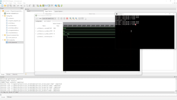
Current FPGA-side implementation is designed for Sipeed Tang chips and the GOWIN toolchain, but it should be portable to an open-source toolchain in the future. Make sure you’re using a USB3 capture card with a MS2130 chipset, load the test code into your FPGA, run the userspace capture side, and you’re ready to add this interface to your FPGA project! It’s well worth it, too – during testing, [Steve] has got data transfer speeds up to 180 MB/s, without the USB3 complexity.
As a test, [Steve] shows us an RX-only SDR project using this interface, with respectable amounts of bandwidth. The presentation goes a fair bit into the low-level details of the protocol, from HDMI fundamentals, to manipulating the MS2130 registers in a way that disables all video conversion; do watch the recording, or at least skim the slides! Oh, and if you don’t own a capture card yet, you really should, as it makes for a wonderful Raspberry Pi hacking companion in times of need.