Molecular beam epitaxy system Veeco Gen II at the FZU – Institute of Physics of the Czech Academy of Sciences. The system is designed for growth of monocrystalline semiconductors, semiconducting heterostructures, materials for spintronics and other compound material systems containing Al, Ga, As, P, Mn, Cu, Si and C.

Germanium Semiconductor Made Superconductor By Gallium Doping

Over on ScienceDaily we learn that an international team of scientists have turned a common semiconductor germanium into a superconductor.

Researchers have been able to make the semiconductor germanium superconductive for the first time by incorporating gallium into its crystal lattice through the process of molecular-beam epitaxy (MBE). MBE is the same process which is used in the manufacture of semiconductor devices such as diodes and MOSFETs and it involves carefully growing crystal lattice in layers atop a substrate.

When the germanium is doped with gallium the crystalline structure, though weakened, is preserved. This allows for the structure to become superconducting when its temperature is reduced to 3.5 Kelvin. Read all about it in the team’s paper here (PDF).

It is of course wonderful that our material science capabilities continue to advance, but the breakthrough we’re really looking forward to is room-temperature superconductors, and we’re not there yet. If you’re interested in progress in superconductors you might like to read about Floquet Majorana Fermions which we covered earlier this year.

A brown plastic circuit board is visible in the middle of the picture, containing an integrated circuit, a resistor, a diode, two capacitors, and some jumper wires going away to the sides.

A Solderless, Soluble Circuit Board

Anyone who’s spent significant amounts of time salvaging old electronics has probably wished there were a way to take apart a circuit board without desoldering it. [Zeyu Yan] et al seem to have had the same thought, and designed circuit boards that can be dissolved and recycled when they become obsolete. Read the details in the research paper. (PDF)

The researchers printed the circuit boards out of water-soluble PVA, with hollow channels in place of interconnects. After printing the boards, they injected a eutectic gallium-indium liquid metal alloy into these channels, populated the boards with components, making sure that their leads were in contact with the liquid alloy, and finally closed off the channels with PVA glue, which also held the components in place. When the board is ready to recycle, they simply dissolve the board and glue in water. The electric components tend to separate easily from the liquid alloy, and both can be recovered and reused. Even the PVA can be reused: the researchers evaporated the solution left after dissolving a board, broke up the remaining PVA, and extruded it as new filament.
Continue reading “A Solderless, Soluble Circuit Board”

Liquid Metal Ion Thrusters Aren’t Easy

What do scanning electron microscopes and satellites have in common? On the face of things, not much, but after seeing [Zachary Tong]’s latest video on liquid metal ion thrusters, we see that they seem to have a lot more in common than we’d initially thought.

As you’d expect with such a project, there were a lot of false starts and dead ends. [Zach] started with a porous-emitter array design, which uses a sintered glass plate with an array of tiny cones machined into it. The cones are coated in a liquid metal — [Zach] used Galinstan, an alloy of gallium, indium, and tin — and an high voltage is applied between the liquid metal and an extraction electrode. Ideally, the intense electric field causes the metal to ionize at the ultra-sharp tips of the cones and fling off toward the extraction electrode and into the vacuum beyond, generating thrust.

Getting that working was very difficult, enough so that [Zach] gave up and switched to a slot thruster design. This was easier to machine, but alas, no easier to make work. The main problem was taming the high-voltage end of things, which seemed to find more ways to produce unwanted arcs than the desired thrust. This prompted a switch to a capillary emitter design, which uses a fine glass capillary tube to contain the liquid metal. This showed far more promise and allowed [Zach] to infer a thrust by measuring the tiny current created by the ejected ions. At 11.8 μN, it’s not much, but it’s something, and that’s the thing with ion thrusters — over time, they’re very efficient.

To be sure, [Zach]’s efforts here didn’t result in a practical ion thruster, but that wasn’t the point. We suspect the idea here was to explore the real-world applications for his interests in topics like electron beam lithography and microfabrication, and in that, we think he did a bang-up job with this project.

Continue reading “Liquid Metal Ion Thrusters Aren’t Easy”

Nanoparticles Rip Hydrogen From Water

Hydrogen fuel is promising, and while there’s plenty of hydrogen in the air and water, the problem is extracting it. Researchers have developed a way to use aluminum nanoparticles to rip hydrogen out of water with no additional energy input. It does, however, require gallium to enable the reaction. The reaction isn’t unknown (see the video below), but the new research has some interesting twists.

Aluminum, of course, is cheap and plentiful. Gallium, not so much, but the process allows recovery and reuse of the gallium, so that makes it more cost-effective. There is a patent pending for the process and — of course — the real trick is making the aluminum nanoparticles. But if you have that, this is a simple way to extract hydrogen from water with no extra energy and at room temperature. Since the reaction of creating aluminum oxide and releasing hydrogen with gallium is pretty well-known, it appears the real research here is determining the optimal properties of the aluminum and the ratio of aluminum to gallium.

While gallium isn’t a common item around the typical hacker’s workshop — unless you count the stuff bound up in semiconductors — it isn’t that expensive and it is relatively easy to handle. Hydrogen, though, not so much — so if you do decide to use this method to produce hydrogen, be careful!

We’ve seen gallium robots and even an antenna. So if you do get some of the liquid metal, there are plenty of experiments to try.

Better Robots Through Gallium

In the movie Terminator 2, the T-1000 robot was made of some kind of liquid metal that could change shape among other interesting things. According to a chemical engineer at North Carolina State University, there may be something to the idea. [Michael Dickey] has been experimenting with gallium, a liquid metal, that scientists think may unlock a new generation of flexible devices.

The most common liquid metal is mercury, of course, and it has its uses. However, its toxicity has led to a reduction in its use. Gallium has low toxicity and also doesn’t easily evaporate. What can you do with it? Check out the video below to see a very simple demonstration of the liquid metal lifting a small — very small — weight with an electrical impulse.

Continue reading “Better Robots Through Gallium”

Silicone Devices: DIY Stretchable Circuits

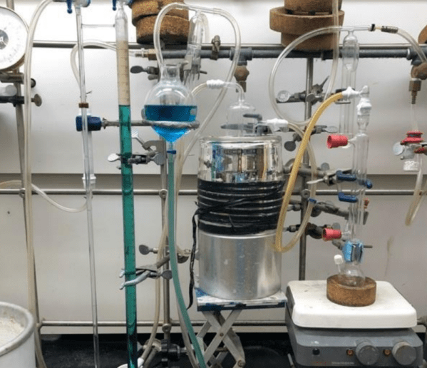
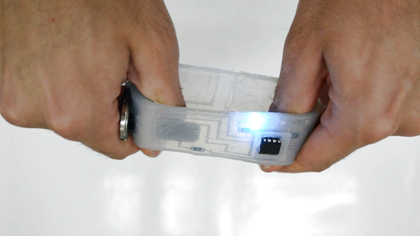
Flexible circuits built on polyimide film are now commonplace, you can prototype with them at multiple factories, at a cost that is almost acceptable to your average hacker. Polyimide film is pretty tough for something so thin, but eventually it will tear, and with larger components, bend radii are quite restricted. But what about stretchable circuits, as in circuits you can flex, twist and stretch? Let us introduce silicone devices. A research group from Hasselt University, Belgium, have been prototyping making truly flexible, silicone-based circuit substrates, managing to integrate a wide range of SMT component types with a dual layer interconnect, with vias and external contacts.

It should be possible to reproduce the process using nothing more special than your average Makerspace CO2 laser cutter, and a couple of special tools that can be easily made — a guide for that is promised — it is purely a matter of gathering a few special materials, and using off-cuts you have lying around for the rest. The interconnect uses Galinstan, which is a low melting point alloy of gallium, indium, and tin. Unfortunately, this material is fairly expensive and cannot be shipped by air due to the gallium content, without specialised handling, at considerable expense. But that aside, other than some acrylic sheets, some vinyl, copper foil and a few sprays, nothing is beyond reach.

The construction process is reverse to what we normally see, with the components and copper contact plates placed first, on to a primed vinyl sheet. This sheet is laser marked with the component outlines to enable them to be corrected placed. Yes, that’s right, they’re using a laser cutter to mark vinyl, a chlorine-containing plastic. Hold on to that thought for a bit.

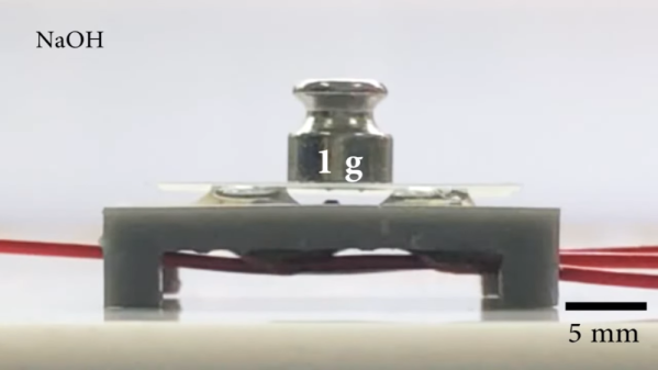
Insulating layers and substrate layers are constructed by blade-coating with a layer of clear silicone. Interconnect layers are formed by sticking a fresh vinyl sheet onto the exposed contacts and laser cutting just though it to expose the pads and the interconnect traces. Next the fancy Galinstan is applied by brush and the vinyl stencil removed. Rinse and repeat for the next layer of insulating silicone, more circuit traces, then use the laser cutter to precisely etch through the via regions to allow more metalisation to be added. Finally a coating of silicone is applied over the whole assembly, the laser is again used to etch the silicone away from the contact pads, and with a little solder tinning of these, you’re done. Simple, if only our Makerspaces didn’t have rules against laser cutting vinyl.

This was clearly a very brief overview, here is a very detailed instructables guide ready for you, as well as a formal research paper, detailing why this came about and why you might want to try this yourself.

If you’re into custom wearables, you might remember this earlier piece about silicone circuits, and this one weird organic-looking thing from the same time-frame.

Continue reading “Silicone Devices: DIY Stretchable Circuits”

Circuit Boards You Can Stretch: Liquid Metal Nanomaterials Make A Strange Flex

If you think polyimide-based flexible PCBs are cool, wait until you get a load of what polymerized liquid metal networks can do.

Seems like [CNLohr] has some pretty cool friends, and he recently spent some time with a couple of them who are working with poly LMNs and finding out what they’re good for. Poly LMNs use a liquid metal composed of indium and gallium that can be sprayed onto a substrate through a laser-cut stencil. This results in traces that show the opposite of expected behavior; where most conductors increase in resistance when stretched, pol LMNs stay just as conductive no matter how much they’re stretched.

The video below shows [CNLohr]’s experiments with the stuff. He brought a couple of traditional PCB-based MCU circuits, which interface easily with the poly LMN traces on a thick tape substrate. Once activated by stretching, which forms the networks between the liquid metal globules, the traces act much like copper traces. Attaching SMD components is as simple as sticking them to the tape — no soldering required. The circuits remain impressively stretchy without any apparent effect on their electrical properties — a characteristic that should prove interesting for wearables circuits, biological sensors, and a host of real-world applications.

While poly LMNs aren’t exactly ready for the market yet, they don’t seem terribly difficult to make, requiring little in the way of exotic materials or specialized lab equipment. We’d love to see someone like [Ben Krasnow] pick this up and run with it — it seems right up his alley.

Continue reading “Circuit Boards You Can Stretch: Liquid Metal Nanomaterials Make A Strange Flex”