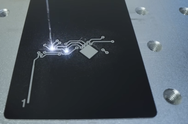
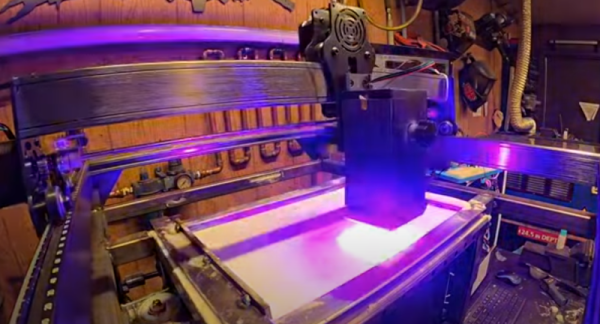
You know you aren’t supposed to watch your laser while it is cutting or engraving. But [Alex] hosted Wired in his studio and showed them how lasers engrave metal with a fiber laser. You can see the video below.
If you haven’t used a fiber laser, you might be surprised that while a 60 W model can burn metal, it does absolutely nothing to [Alex’s] hand. We wouldn’t try that, by the way, with the common diode lasers you see in most hacker’s labs these days. The video isn’t terribly technical, but it is interesting to see different metals succumb to the powerful laser. There are a few tips about marking different metals in different ways and how to deal with thermal expansion and other effects.
Fiber lasers aren’t as common as diode engravers in private shops, but we assume it is just a matter of time before they get cheaper. Not to mention their widespread use commercially means surplus units might become available, too.
If you are interested in lasers, [Alex’s] YouTube channel has quite a few interesting videos to check out. If you need more power, how’s 200 kW? Then again, even 20 W will get you something useful.

