Readers who survived the 1970s will no doubt remember the “mood ring” fad, where a liquid crystal mounted to a ring would magically reveal your current emotional state to all and sundry by changing color. This nifty thermochromic display is based on the same principle, and while it might not start a new craze, it’s still pretty mesmerizing to watch.
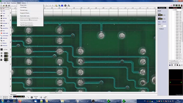
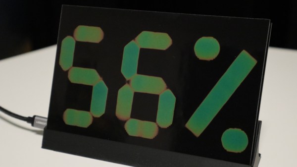
This isn’t [Moritz v. Sivers]’ first attempt at a thermochromic display. His earlier version was far more complicated, using separate copper plates clad with thermochromic film for each segment, with Peltier devices to cool and heat them individually. Version two is much simpler, using a printed circuit board with heating elements in the shape of seven-segment displays etched into it. The thermochromic film sits directly on the heater PCB; a control PCB below has the MCU and sensors on it. The display alternates between temperature and humidity, with the segments fading in an uneven and ghostly way that really makes this fun to watch. [Moritz] has made the build files available, and there’s a detailed Instructable as well.
We’re always on the lookout for alternate display modalities, especially when they look this cool. We’ve seen other thermochromic displays before, of course, and persistence of phosphorescence looks great, too.
Continue reading “Thermochromic Display Tells You The Temperature Despite Your Current Mood”