These days, PCB fab houses are just about everywhere, and you can’t go buy a taco without walking past eight of them. Still, some out there still like to etch their PCBs at home. If that sounds like you, you might see some value in [Chris Borge]’s PCB agitator.
The design mostly relies on 3D printed parts, including the main body. It has a heavy base which is filled with concrete to keep it nicely weighed down on the table. A table for holding a PCB and fluid tank is then installed on top, via a bearing which allows it to pivot in one axis. An Arduino Nano commands the agitation of the table top, and hence the PCB etching tank, with a servo used to actually shift the table back and forth.
It’s a simple design — far simpler than some of the advanced coffee-making hardware we’ve seen recently. Regardless, it gets the job done, and done well! In testing, it accelerated [Chris]’s etching jobs significantly, we’re talking hours here. Meanwhile, if you don’t have a 3D printer on hand, you could always try building one out of junk instead!
For vintage calculator fans, nothing strikes more fear than knowing that someday their precious and irreplaceable daily driver will become a museum piece to be looked at and admired — but never touched again. More often than not, the failure mode will be the keypad.
In an effort to recover from the inevitable, at least for 70s vintage TI calculators, [George] has come up with these nice replacement keypad PCBs. The original membrane switches on these calculators have a limited life, but luckily there are ultra-slim SMD tactile switches these days make a dandy substitute. [George] specifies a 0.8 mm thick switch that when mounted on a 1.6 mm thick PCB comes in just a hair over the original keypad’s 2.2 mm thickness. He has layouts for a TI-45, which should also fit a TI-30, and one for the larger keypads on TI-58s and TI-59s.
While these particular calculators might not in your collection, [George]’s goal is to create an open source collection of replacement keypads for all the vintage calculators sitting in desk drawers out there. And not just keypads, but battery packs, too.
Printed circuit boards are typically only something you’d find in a digital watch. However, as [IndoorGeek] demonstrates, you can put them to wonderful use in a classical analog watch, too. They can make the perfect watch dial!
Here’s the thing. A printed circuit board is fundamentally some fiberglass coated in soldermask, some copper, maybe a layer of gold plating, and with some silk screen on top of that. As we’ve seen a million times, it’s possible to do all kinds of artistic things with PCBs; a watch dial seems almost obvious in retrospect!
[IndoorGeek] steps through using Altium Designer and AutoCAD to layout the watch face. The guide also covers the assembly of the watch face into an actual wrist watch, including the delicate placement of the movement and hands. They note that there are also opportunities to go further—such as introducing LEDs into the watch face given that it is a PCB, after all!
It’s a creative way to make a hardy and accurate watch face, and we’re surprised we haven’t seen more of this sort of thing before. That’s not to say we haven’t seen other kinds of watch hacks, though; for those, there have been many. Video after the break.
[Hans Rosenberg] knows a thing or two about RF PCB design and has provided a three-part four-part video demonstration of some solid rules of thumb. We will cover the first part here and leave the other two for the more interested readers!
The design process begins with a schematic diagram, assuming ideal conductors. Advanced software tools can extract the resistive, inductive, and capacitive elements of the physical wiring to create a parasitic model that can be compared to the desired schematic. The RF designer’s task is to optimize the layout to minimize differences and achieve the best performance to meet the design goals. However, what do you do when you don’t have access to such software?
[Hans] explains that at low frequencies, return current flows through all paths, with the lowest resistance path taking most of the current. At higher frequencies, the lowest inductance path carries all the current. In real designs, a ground plane is used instead of an explicit return trace for the lowest possible impedance.
You really wouldn’t design an RF circuit like this.
[Hans] shows the effect of interrupting the signal return path on a physical test PCB. The result is pretty bad, with the current forced to detour around the hole in the ground plane. A nanoVNA shows a -20 dB drop at 4 GHz, where the ground plane has effectively become an antenna. Energy will be radiated out, causing signal loss, but worse, it will create an EMC hazard with an unintended transmission.
Additionally, this creates an EMC susceptibility, making the situation worse. Placing a solder blob to bridge the gap directly under the signal trace is all that’s required to make it a continuous straight path again, and the performance is restored.
Floating planes are also an issue in RF designs, causing signal resonance and losses. One solution is to pull back the planes near the signal or stitch them to the ground plane with vias placed closely on either side of the signal trace. However, such stitching may slightly affect transmission line impedance and require tweaking the design a little. The next two parts of the series expand on this, hammering home the importance of good ground plane design. These are definitely worth a watch!
When thinking of the first PCs, most of us might imagine something like the Apple I or the TRS-80. But even before that, there were a set of computers that often had no keyboard, or recognizable display beyond a few blinking lights. [Artem Kalinchuk] is attempting to recreate one of these very early digital computers, the Kenbak-1, using as many period-correct parts as possible.
Considered by many to be the world’s first personal computer, the Kenbak-1 was an 8-bit machine with 256 bytes of memory, using TTL integrated circuits for the logic as there was no commercially available microprocessor available at the time it was designed. For [Artem]’s build, most of these parts can still be sourced including the 7400-series chips and carbon resistors although the shift registers were a bit of a challenge to find. A custom PCB was built to replicate the original, and with all the parts in order it’s ready to be assembled and put into a case which was built using the drawings for the original unit.
Although [Artem] plans to build a period-correct linear power supply for this computer, right now he’s using a modern switching power supply for testing. The only other major components that are different are the status lamps, in this case switched to LEDs because he wasn’t able to source incandescent bulbs that drew low enough current, and the switches which he’s replaced with MX-style keys. We’ll stay tuned as he builds and tests this over the course of several videos, but in the meantime if you’re curious how this early computer actually worked we featured an emulator for it a while back.
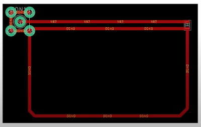
Ordering a PCB? Two of them? Three? Five? For about eight years now, I’ve been regularly ordering large numbers of different PCBs, and, naturally, have developed a toolkit to make things smoother. One trick is PCB panelization, and you should really know about it.
You might’ve encountered PCB panels already. Perhaps, if you order PCBA at a fab, you will get your board returned in a whole new form-factor, with rails on the sides that you have to snap off before your PCB is usable. Those rails are used so that your PCBs are easier to handle during assembly, but that’s far from the only reason why you would make a panel.
If you need multiple pieces of a PCB, your fab may say that building 50 pcs is classified as “large batch” and that takes longer than 30 days, which delays your entire PCB order. I’ve been there, five years ago, running out of time right before Chinese New Year. The fix was simple – I made a 2×2 panel and ordered that in quantity of 10-15. Panelization might be a little more expensive, or maybe even cheaper, but, most importantly, it will be faster.
In a few hours’ time, I sat down, figured out that KiCad has built-in features for panelization, and ordered panels instead of separate PCBs. Thanks to that, I made the Chinese New Year deadline that year and could successfully restock my store, letting me earn a fair bit of money instead of keeping a popular product out-of-stock – ultimately, helping my family stay up on rent that month.
Panelization lets you hack around many PCB ordering and assembly limitations, and I’ve only gotten started – there’s way way more! For now, let’s sort out panelizing multiples of the same PCB. As long as your boards are using KiCad (or KiCad-converted from Eagle/EasyEDA/Altium/gerbers), there’s no better software than KiKit.
When everything used wires, it was easy to splice them or replace them. Not so much with PC boards, but everyone has their favorite method for repairing a broken trace. [Mr. SolderFix] has his five favorite ways, as you can see in the video below.
Of course, before you can repair a trace, you probably have to expose it since most boards have solder mask now. Unless you plan to shut the trace at both ends, exposing the actual trace is probably the first step.