Modern display and solar cell technologies are built with a material called Indium Tin Oxide (ITO). ITO has excellent optical transparency and electrical conductivity, and the material properties needed for integration in large-scale manufacturing. However, we’re not content with just merely “good enough” nowadays, and need better materials to build ever better devices. Graphene and carbon nanotubes have been considered as suitable replacements, but new research has identified a different possibility: nanowires.
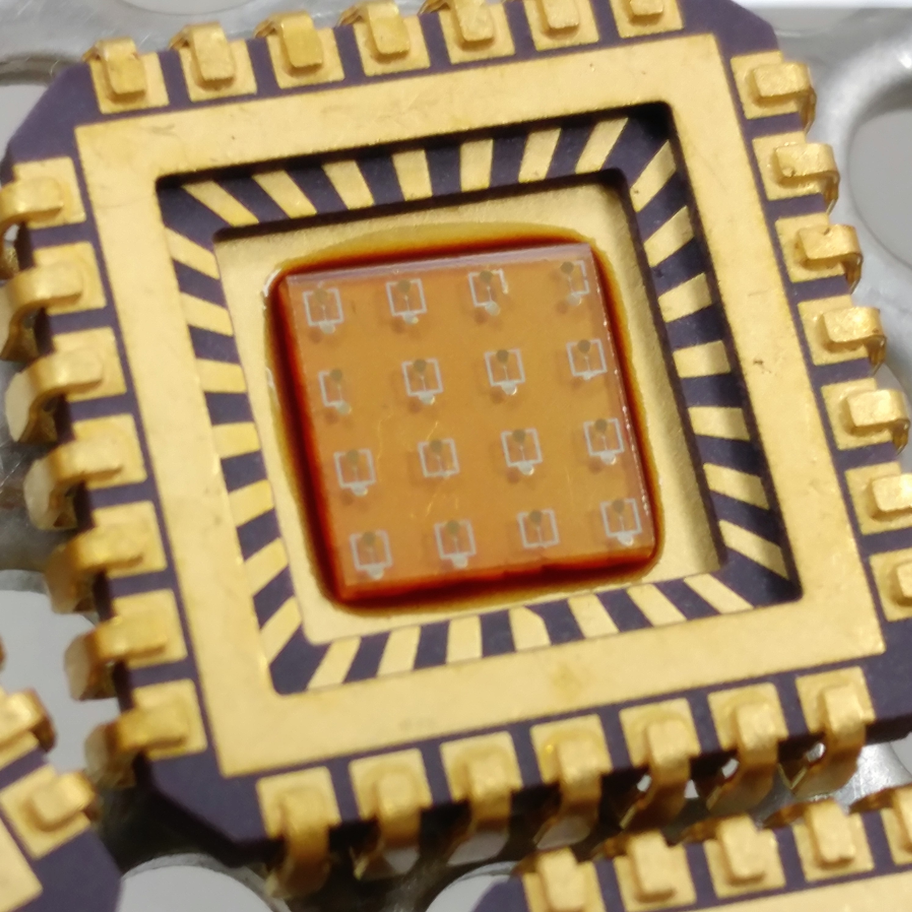
Researchers from the Indian Association for the Cultivation of Science (IACS) and the Centre for Research on Adaptive Nanostructures and Nanodevices (CRANN) in Ireland have demonstrated a seamless silicon nanowire junction that can be used for photodetector and display technology.
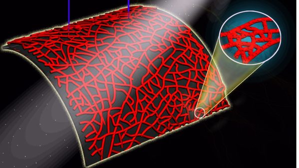
Before you get lost in the jargon, let’s take a step back. A nanowire is just a very narrow length of wire, on the order of 1 nanometer across. When silicon is used at this scale, electrical charges can become stuck (called “charge trapping”), which means that the holes and electrons are separated, allowing for transistors and photovoltaics. By controlling where these holes form in the nanowire, you can create a “seamless” junction without using any dopant materials to create impurities, as is done in modern CMOS transistors
These material properties allow the functionality of a junction, but it still needs to be easily and repeatably manufactured. To solve this problem, the team put the nanowire transistors on a flexible polymer, which should enable flexible nanowire applications, such as a roll-up screen.
The first step towards a display is a simple photodetector, just consisting of a basic P-N junction, but they hope this technology will eventually be useful in “smart windows” due to the junctions’ applicability to photodetectors and cameras. Moving to emitting light for displays or creating a solar cell using this technology will probably take some time.
Do you have any experience with different materials for creating junctions? What would you do with a small, transparent photodetector? We’ve featured homebrew solar cells before, as well as creating DIY semiconductors. We’ve also seen silver nanowires for wearable circuits.
[Via IEEE Spectrum]