Persistent Displays With UV Light

This year’s Hackaday Prize has “Rethink Displays” as one of its first theme, and [Tucker Shannon] has given us his best shot on that subject with a set of impressive displays that “write” on glow-in-the-dark material using ultra-violet light. These materials glow for a while after UV illumination, so moving a light source like a UV LED over the surface draws glowing text or simple graphics which can be readily consumed.

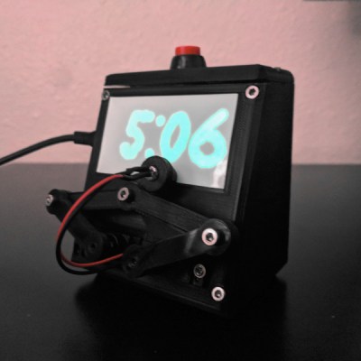
One of the examples this a clock we were first smitten with back in 2018. It is a rather attractive 3D-printed affair with those servos mounted below the screen that moves a UV LED through a pair of linkages. Other offerings that play on the same UV stylus medium include a laser on an az-el mount controlled by a Raspberry Pi Zero. It’s a neat idea very effectively done, and we can see it has a lot of potential.

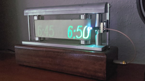
But the most impressively advanced so far is the model shown in the image at the top of the article and the demo video at the bottom. A loop of phosphorescent material is the display surface itself. This one moves that loop with two rollers to make up the X axis, and moves the UV source up and down for the Y axis. As with all of these designs, whatever is written will soon fade, leaving the surface ready for the next bit of information.

Interested in this project and think you could do a display of your own? The Hackaday Prize 2021 is live, and we’d love to see you enter it!

Continue reading “Persistent Displays With UV Light”

Cocktail Of Chemicals Makes This Blueprint Camera Unique

When you’re looking at blueprints today, chances are pretty good that what you’re seeing is anything but blue. Most building plans, diagrams of civil engineering projects, and even design documents for consumer products never even make it to paper, let alone get rendered in old-fashioned blue-and-white like large-format prints used to produced. And we think that’s a bit of a shame.

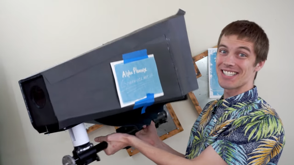
Luckily, [Brian Haidet] longs for those days as well, so much so that he built this large-format cyanotype camera to create photographs the old-fashioned way. Naturally, this is one of those projects where expectations must be properly scaled before starting; after all, there’s a reason we don’t go around taking pictures with paper soaked in a brew of toxic chemicals. Undaunted by the chemistry, [Brian] began his journey with simple contact prints, with Sharpie-marked transparency film masking the photosensitive paper, made from potassium ferricyanide, ammonium dichromate, and ammonium iron (III) oxalate, from the UV rays of the sun. The reaction creates the deep, rich pigment Prussian Blue, contrasting nicely with the white paper once the unexposed solution is washed away.

[Brian] wanted to go beyond simple contact prints, though, and the ridiculously large camera seen in the video below is the result. It’s just a more-or-less-lightproof box with a lens on one end and a sheet of sensitized paper at the other. The effective ISO of the “film” is incredibly slow, leading to problematically long exposure times. Coupled with the distortion caused by the lens, the images are — well, let’s just say unique. They’ve got a ghostly quality for sure, and there’s a lot to be said for that Prussian Blue color.

We’ve seen cyanotype chemistry used with UV lasers before, and large-format cameras using the collodion process. And we wonder if [Brian]’s long-exposure process might be better suited to solargraphy.

Continue reading “Cocktail Of Chemicals Makes This Blueprint Camera Unique”

Laser Blasts Out High-Quality PCBs

With how cheap and how fast custom PCBs have gotten, it almost doesn’t make sense to roll your own anymore, especially when you factor in the messy etching steps and the less than stellar results. That’s not the only way to create a PCB, of course, and if you happen to have access to a 20-Watt fiber laser, you can get some fantastic homemade PCBs that are hard to tell from commercial boards.

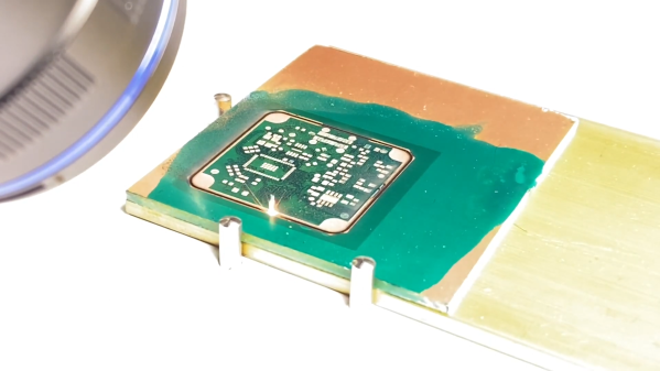
Lucikly, [Saulius Lukse] of Kurokesu fame has just such a laser on hand, and with a well-tuned toolchain and a few compromises, he’s able to turn out 0.1-mm pitch PCBs in 30 minutes. The compromises include single-sided boards and no through-holes, but that should still allow for a lot of different useful designs. The process starts with Gerbers going through FlatCAM and then getting imported into EZCAD for the laser. There’s a fair bit of manual tweaking before the laser starts burning away the copper between the traces, which took about 20 passes for 0.035-mm foil on FR4. We have to admit that watching the cutting proceed in the video below is pretty cool.

Once the traces are cut, UV-curable solder resist is applied to the whole board. After curing, the board goes back to the laser for another pass to expose the pads. A final few passes with the laser turned up to 11 cuts the finished board free. We wonder why the laser isn’t used to drill holes; we understand that vias would be hard to connect to the other side, but it seems like through-hole components could be supported. Maybe that’s where [Saulius] is headed with this eventually, since there are traces that terminate in what appears to be via pads.

Whatever the goal, these boards are really slick. We usually see lasers used to remove resist prior to traditional etching, so this is a nice change.

Continue reading “Laser Blasts Out High-Quality PCBs”

A UV Curing Wand For Everyone

The average person’s experience with an ultraviolet (UV) wand is getting a cavity at the dentist. However, anyone with a resin-based 3d printer knows how important a UV curing system is. Often times some spots on a print need a little bit of extra UV to firm up. [Mile] has set out to create an open-source UV curing wand named Photon that is cost-effective and easy to build.

What’s interesting here is that there are dozens if not hundreds of UV curing systems ranging from $5 LED flashlights to larger industrial flood systems. [Mile] dives right in and shows the trade-offs that those cheaper modules are making as well as what the commercial systems are doing that he isn’t. [Mile’s] Photon wand tries to be energy efficient with more irradiated power while staying at a lower cost. This is done by carefully selecting the CSP LEDs instead of traditional wire-bonded and making sure the light source is properly focused and cooled. From the clean PCB and slick case, it is quite clear that [Mile] has gone the extra step to make this production-friendly. Since there are two industry-standard wavelengths that resins cure at (364nm and 405nm), the LED modules in Photon are user-replaceable.

What we love about this project is looking past what is readily available and diving deep. First understanding the drawbacks and limitations of what is there, then setting a goal and pushing through to something different. This isn’t the first UV curing tool we’ve seen recently, so it seems there is a clear need for something better that’s what is out there today.

Continue reading “A UV Curing Wand For Everyone”

UVA Aims To Be More Than Just One Tool

Sometimes, a project is more than it seems on just the surface. The UVA project from [Said Alvarado Marin] is one such example. What started as an attempt to build a single useful tool became the beginning of a broader utility ecosystem.

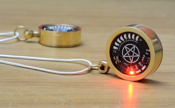
In and of itself, UVA is a project to build a powerful UV flashlight for curing UV-reactive glues. After some serious research, [Said] was able to find the right LEDs, outputting the right wavelengths, and begin the design of this simple tool. However, UVA quickly became a base upon which other tools could be developed. The design of UVA is such that the flashlight head fits onto an interchangable power base, consisting of three 18650 lithium polymer cells and a charging subsystem.

The aim of UVA is to encourage others to produce their own tools to work with this ecosystem. Designed around commonly available parts and DIY build methods like 3D printing, it’s intended to allow the average person to create the tools they need when and as they need them, on location. We look forward to seeing how the project progresses further as we head closer to the finale of the 2020 Hackaday Prize!


A PIN Pad Blasting UV Sanitizer

Retailers have instituted enhanced cleaning procedures in response to the COVID-19 pandemic, with an aim to keep frequently touched surfaces as clean as possible. Certainly one of the most commonly handled objects in the entire store is the payment terminal by the register, and the PIN pad specifically. Which is why [Josh Starnes] is working on a UV sterilizer that mounts onto a standard credit card terminal.

It’s a simple enough idea, but as is often the case, figuring out how to properly execute it is where things get tricky. [Josh] has already moved through several design iterations for his 3D printed enclosure in an attempt to make something that’s unobtrusive enough to be practical. The goal is to make something that the user won’t mistake for some kind of skimming device, which can certainly be tricky.

The skeptics in the audience will be happy to hear that [Josh] isn’t bothering with an LED UV source, either. We’ve all seen the pitfalls of trying to sanitize using UV LEDs, so this design goes old school with a small 12 volt UV bulb. That does mean it will need a dedicated power source however, which it seems like he’ll be addressing in the next phase of the project.


Printing, Plating, And Baking Makes DIY Microlattices Possible

To be honest, we originally considered throwing [Zachary Tong]’s experiments with ultralight metallic microlattices into the “Fail of the Week” bucket. But after watching the video below for a second time, it’s just not fair to call this a fail, so maybe we’ll come up with a new category — “Qualified Success of the Week”, perhaps?

[Zachary]’s foray into the strange world of microlattices began when he happened upon a 2011 paper on the subject in Science. By using a special photocurable resin, the researchers were able to use light shining through a mask with fine holes to create a plastic lattice, which was then plated with nickel using the electroless process, similar to the first half of the electroless nickel immersion gold (ENIG) process used for PCBs. After removing the resin with a concentrated base solution, the resulting microlattice is strong, stiff, and incredibly light.

Lacking access to the advanced materials and methods originally used, [Zachary] did the best he could with what he had. An SLA printer with off-the-shelf resin was used to print the skeleton using the same algorithms used in the original paper. Those actually turned out pretty decent, but rather than electroless plating, he had to go with standard electroplating after a coat of graphite paint. The plated skeletons looked great — until he tried to dissolve the resin. When chemical approaches failed, into the oven went the plated prints. Sadly, it turns out that the polymers in the resin expand when heated, which blew the plating apart. A skeleton in PLA printed on an FDM printer fared little better; when heated to drive out the plastic, it became clear that the tortuous interior of the lattice didn’t plate very well.

From aerogels to graphene, we love these DIY explorations of new and exotic materials, so hats off to [Zachary] for giving it a try in the first place.

Continue reading “Printing, Plating, And Baking Makes DIY Microlattices Possible”