M8SBC-86 Is An FPGA-Based “Kinda PC Compatible” 486 SBC

Given the technical specs of the FPGAs available to hobbyists these days, it really shouldn’t be a shock that you can implement a relatively-modern chipset on one, like one for a 486 system. In spite of knowing that in the technical sense, we were still caught off guard by [maniek-86]’s M8SBC project that does just that– the proas both CPU and BIOSducing a 486 FPGA chipset with a motherboard to boot.

Boot what? Linux 2.2.6, MS-DOS 6.22 or FreeDOS all work. It can run DOOM, of course, along with Wolfenstien 3D, Prince of Persia, and even the famous Second Reality demo– though that last without sound. [maniek-86]’s implementation is lacking direct memory access, so sound card support is right out. There are a few other bugs that are slowly being squished, too, according to the latest Reddit thread. Continue reading “M8SBC-86 Is An FPGA-Based “Kinda PC Compatible” 486 SBC”

6502 Goes FPGA (Again)

While there has been no shortage of FPGA-based recreations of classic processors, we always enjoy seeing a new approach. Last month [Some Assembly Required] took on the challenge to recreate a classic computer from the ground up and started with a 6502 implementation in Verilog. You can see in the second video below that he’s made good progress and there are apparently more videos to come.

The ROL instruction is the subject of the second video. We liked the approach of looking at what the instruction does and how many cycles it takes on different variants It is always good to make sure you know exactly what you are trying to accomplish before you get started.

Continue reading “6502 Goes FPGA (Again)”

Raspberry Pi Real-Time HAT

New Part Day: Raspberry Pi HAT For IEEE1588 Precision Time Protocol

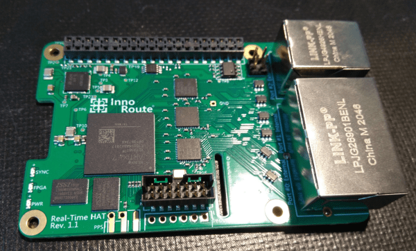
The new Real-Time HAT by InnoRoute adds IEEE1588 PTP support in hardware to a Raspberry Pi 4 nestled beneath. Based around a Xilinx Artix-7 FPGA and a handful of gigabit Ethernet PHY devices, the HAT acts as network-passthrough, adding accurate time-stamps to egress (outgoing) packets and stripping time-stamps from the ingress (incoming) side.

This hardware time-stamping involves re-writing Ethernet packets on-the-fly using specialised network hardware which the Raspberry Pi does not have. Yes, there are software-only 1588 stacks, but they can only get down to 10s of microsecond resolutions, unlike a hardware approach which can get down to 10s of nanoseconds.

1588 is used heavily for applications such as telecoms infrastructure, factory equipment control and anything requiring synchronisation of data-consuming or data-producing devices. CERN makes very heavy use of 1588 for its enormous arrays of sensors and control equipment, for all the LHC experiments. This is the WhiteRabbit System, presumably named after the time-obsessed white rabbit of Alice In Wonderland fame. So, if you have a large installation and a need for precisely controlling when stuff happens across it, this may be just the thing you’re looking for.

IEEE1588 PTP Synchronisation

The PTP client and master device ping a few messages back and forth between themselves, with the network time-stamper recording the precise moment a packet crosses the interface. These time-stamps are recorded with the local clock. This is important. From these measurements, the time-of-flight of the packet and offset of the local clock from the remote clock may be calculated and corrected for. In this way each client node (the hat) in the network will have the same idea of current time, and hence all network packets flowing through the whole network can be synchronised.

The beauty of the system is that the network switches, wiring and all that common infrastructure don’t need to speak 1588 nor have any other special features, they just need to pass along the packets, ideally with a consistent delay.

The Real-Time HAT configures its FPGA via SPI, straight from Raspberry Pi OS, with multiple applications possible, just by a change on the command line. It is possible to upload custom bitstreams, allowing the HAT to be used as a general purpose FPGA dev board should you wish to do so. It even stacks with the official PoE HAT, which makes it even more useful for hanging sensors on the end of a single wire.

Of course, if your needs are somewhat simpler and smaller in scale than a Swiss city, you could just hack a GPS clock source into a Raspberry Pi with a little soldering and call it a day.

AMD Acquires Xilinx For $35 Billion

News this morning that AMD has reached an agreement to acquire Xilinx for $35 Billion in stock. The move to gobble up the leading company in the FPGA industry should come as no surprise for many reasons. First, the silicon business is thick in the age of mergers and acquisitions, but more importantly because AMD’s main competitor, Intel, purchased the other FPGA giant Altera back in 2015.

Primarily a maker of computer processors, AMD expands into the reconfigurable computing market as Field-Programmable Gate Arrays (FPGA) can be adapted to different tasks based on what bitstream (programming information written to the chips) has been sent to them. This allows the gates inside the chip to be reorganized to perform different functions at the hardware level even after being put into products already in the hands of customers.

Xilinx invented the FPGA back in the mid-1980s, and since then the falling costs of silicon fabrication and the acceleration of technological advancement have made them evermore highly desirable solutions. Depending on volume, they can be a more economical alternative to ASICs. They also help with future-proofing as technology not in existence at time of manufacture — such as compression algorithms and communications protocols — may be added to hardware in the field by reflashing the bitstream. Xilinx also makes the Zynq line of hybrid chips that contain both ARM and FPGA cores in the same device.

The deal awaits approval from both shareholders and regulators but is expected to be complete by the end of 2021.

What’s Inside An FPGA? Ken Shirriff Has (Again) The Answer

FPGAs are somewhat the IPv6 of integrated circuits — they’ve been around longer than you might think, they let you do awesome things that people are intrigued by initially, but they’ve never really broke out of their niches until rather recently. There’s still a bit of a myth and mystery surrounding them, and as with any technology that has grown vastly in complexity over the years, it’s sometimes best to go back to its very beginning in order to understand it. Well, who’d be better at taking an extra close look at a chip than [Ken Shirriff], so in his latest endeavor, he reverse engineered the very first FPGA known to the world: the Xilinx XC2064.

If you ever wished for a breadboard-friendly FPGA, the XC2064 can scratch that itch, although with its modest 64 configurable logic blocks, there isn’t all that much else it can do — certainly not compared to even the smallest and cheapest of its modern successors. And that’s the beauty of this chip as a reverse engineering target, there’s nothing else than the core essence of an FPGA. After introducing the general concepts of FPGAs, [Ken] (who isn’t known to be too shy to decap a chip in order to look inside) continued in known manner with die pictures in order to map the internal components’ schematics to the actual silicon and to make sense of it all. His ultimate goal: to fully understand and dissect the XC2064’s bitstream.

Of course, reverse engineering FPGA bitstreams isn’t new, and with little doubt, building a toolchain based on its results helped to put Lattice on the map in the maker community (which they didn’t seem to value at first, but still soon enough). We probably won’t see the same happening for Xilinx, but who knows what [Ken]’s up to next, and what others will make of this.

Xilinx Makes MIPI CSI And DSI Controller IP Blocks Free To Use With Vivado

If you want to use a display or camera with an FPGA, you will often end up with a MIPI-based solution. As of the Xilinx Vivado 2020.1 release, the MIPI DSI (display serial interface) and CSI (camera serial interface) IP blocks are now bundled with the IDE to be used freely with Xilinx FPGAs.

The Xilinx MIPI CSI2 receiver block implements the CSI-2 v1.1 specification, which although a bit older is essentially the same CSI implementation as on the Raspberry Pi boards. This means that it would allow one to use this IP block on an FPGA with many common CSI camera modules out there. The IP block offers a standard AXI4 interface for connecting up to the rest of a design.

Similarly, the Xilinx MIPI DSI transmitter block implements DSI v1.3 specification. This offers a maximum data rate of 1.5 Gbps, with an AXI4-lite interface to communicate with the rest of the design. Both IP blocks are subject to the Core license agreement, which doesn’t appear to preclude it from being used in a specific fashion, whether commercial or personal.

This is not the only way to use MIPI devices with an FPGA, of course. Take for example [Daveshah]’s CSRIx project on Github.

Header image: Kwapix / CC BY-SA 4.0

WiFi Goes Open

For most people, adding WiFi to a project means grabbing something like an ESP8266 or an ESP32. But if you are developing your own design on an FPGA, that means adding another package. If you are targeting Linux, the OpenWifi project has a good start at providing WiFi in Verilog. There are examples for many development boards and advice for porting to your own target on GitHub. You can also see one of the developers, [Xianjun Jiao], demonstrate the whole thing in the video below.

The demo uses a Xilinx Zynq, so the Linux backend runs on the Arm processor that is on the same chip as the FPGA doing the software-defined radio. We’ll warn you that this project is not for the faint of heart. If you want to understand the code, you’ll have to dig into a lot of WiFi trivia.

Continue reading “WiFi Goes Open”