Too Much Over-optimization Is Never Enough!

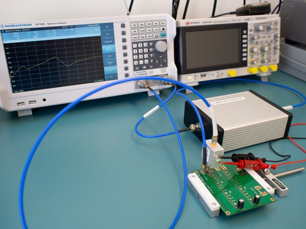
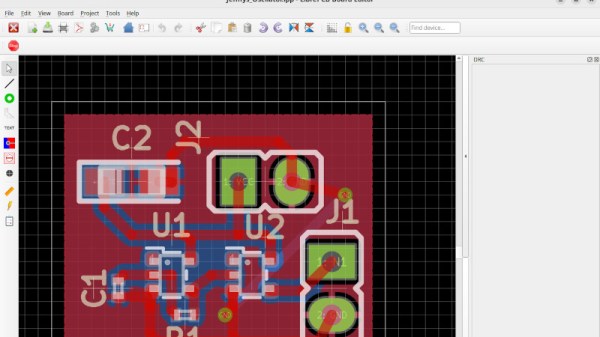
A discussion came up on the Hackaday Discord PCB design channel about resistor networks, and it got me thinking about whether we (the hacker community) use them in designs or not. These handy devices often take the shape of an IC, SMD or otherwise, but between the pins are a bunch of resistors instead of active silicon. They come in all sorts of configurations and tolerances, but the point is usually the same: When you need a bunch of similar resistors, it’s cheaper to go with a network package.

But how much cheaper? I did a quick search for 1 kΩ resistors and the corresponding network, and came up with similar prices for the resistors and networks – but the network has eight resistors in it! That’s an eightfold savings! Which, at a price of roughly one cent per piece, is less than a dime. While it’s certainly true that if you’re making a million widgets, saving a penny per widget matters. But do you spend the time to optimize your projects down to such margins? I want to say “of course not!” but maybe you do?

For me, worrying about seven cents in a PCB design that I may make ten of is foolishness. But still, I’ve used resistor networks for their other side effects: the resistors in a common package tend to be very tightly matched, even if their overall tolerance isn’t. If you’re making something like an R-2R DAC, that’s a definite advantage. Or if you’re space constrained, or just hate placing lots of tiny resistors, the networks shine.

I often forget about resistor networks, and when I do think of them, I think of them in terms of cost savings in industrial applications. But maybe that’s not fair – maybe they do have their hacker uses as well. Are there other parts like this that we should all know about?

Check Your Board: Call For Submissions

As both beginning hackers and Silicon Valley investors alike keep discovering, there are a lot of differences between hardware and software. One important difference is cost of iterating over a design. In software, you can comfortably rerun your build process and push updates out near instantly to tons of users. In hardware, all of that costs money, and I do mean, it costs way more money than you’d want to spend.

When I see people order boards that could never work because of some fundamental design assertions, with mistakes entirely preventable, it hurts. Not in an “embarrassment” way – it’s knowing that, if they asked someone to take a look at the design, they could’ve received crucial feedback, pulled the traces on the board differently or added some components, and avoided spending a significant chunk of money and time expecting and assembling a board that has a fundamental mishap.

Every thing like this might set a beginner back on their hacker journeys, or just have them spend some of their valuable time, and we can do a ton to prevent that by simply having someone experienced take a look.

Continue reading “Check Your Board: Call For Submissions”

Vectorscope KiCad Redrawing Project

When I saw this year’s Supercon Vectorscope badge, I decided that I had to build one for myself. Since I couldn’t attend in-person, I immediately got the PCBs and parts on order. Noting that the GitHub repository only had the KiCad PCB file and not the associated schematics and project file, I assumed this was because everyone was in a rush during the days leading up to Supercon weekend. I later learned, however, that there really wasn’t a KiCad project — the original design was done in Circuit Maker and the PCB was converted into KiCad. I thought, “how hard can this be?” and decided to try my hand at completing the KiCad project.

Fortunately I didn’t have to start from scratch. The PCB schematics were provided, although only as image files. They are nicely laid out and fortunately don’t suffer the scourge of many schematics these days — “visual net lists” that are neither good schematics nor useful net lists. To the contrary, these schematics, while having a slightly unorthodox top to bottom flow, are an example of good schematic design. Continue reading “Vectorscope KiCad Redrawing Project”

Try It Out

It’s like Star Wars versus Star Trek at a SciFi convention, or asking creamy or chunky at the National Peanut Butter Appreciation Festival. (OK, we made that one up.) When Jenny reviewed the 1.0 version of LibrePCB, it opened the floodgates. Only on Hackaday!

Of course it makes sense that in a community of hardware hackers, folks who are not unfamiliar with the fine art and engineering of designing their own PCBs, have their favorite tools. Let’s face it, all PCB design software is idiosyncratic, and takes some learning. But the more fluent you are with your tool of choice, the more effort you have invested in mastering it, leading to something like the sunk-cost phenomenon: because you’ve put so much into it, you can’t think of leaving it.

The beauty of open-source software tools is that there’s almost nothing, aside from your own psychology, stopping you from picking up another PCB program, kicking the proverbial tires with a simple design, and seeing how it works for you. That’s what Jenny did here, and what she’s encouraged me to do. Whether it’s beginner-friendly Fritzing (also recently in version 1.0), upstarts LibrePCB or Horizon EDA, heavyweight champion KiCAD, or the loose-knit conglomeration of tools in coralEDA, you have enough choices that something is going to fit your PCB hand like a glove.

I certainly wouldn’t risk a swap up to a new tool on something super complicated, or something with a tight deadline, but why not start up a fun project to test it out? Maybe follow Tom Nardi’s lead and make a Simple Add-on, for a badge or just as a blinky to put on your desk? Don’t be afraid to try something new!

Review: LibrePCB Hits Version 1.0

Nearly three years ago at the start of 2020 and before the pandemic hit, we took a look at an up-and-coming player in the world of PCB design. LibrePCB is by no means as old as the more established players, but at the time it was joining the ranks of open-source EDA packages with its first early stable releases. It showed a lot of promise but was still a little rough around the edges back then, but in the years since it’s advanced to the extent that in September they released version 1.0. That’s a significant moment for any open source package, so it’s time to return and take another look. It’s a cross-platform package with builds available for Linux, Windows, MacOS and FreeBSD, of which I needed the Linux version. There are one or two options to choose from, I went for the appImage as probably the least trouble. Very quickly I was in a new EDA package, and I set out to make a simple Schmitt trigger oscillator as a test project. Continue reading “Review: LibrePCB Hits Version 1.0”

PCIe For Hackers: Our M.2 Card Is Done

We’ve started designing a PCIe card last week, an adapter from M.2 E-key to E-key, that adds an extra link to the E-key slot it carries – useful for fully utilizing a few rare but fancy E-key cards. By now, the schematic is done, the component placement has been figured out, and we only need to route the differential pairs – should be simple, right? Buckle up.

Getting Diffpairs Done

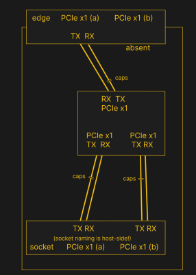
PCIe needs TX pairs connected to RX on another end, like UART – and this is non-negotiable. Connectors will use host-side naming, and vice-versa. As the diagram demonstrates, we connect the socket’s TX to chip’s RX and vice-versa; if we ever get confused, the laptop schematic is there to help us make things clear. To sum up, we only need to flip the names on the link coming to the PCIe switch, since the PCIe switch acts as a device on the card; the two links from the switch go to the E-key socket, and for that socket’s purposes, the PCIe switch acts as a host.

While initially routing this board, I absolutely forgot about one more important thing for PCIe – series capacitors on every data pair, on the host TX side of the link. We need three capacitor pairs here – on TX of the PCIe switch uplink, and two pairs on TX side of the switch – again, naming is host-side. I only remembered this after having finished routing all the diffpairs, and, after a bit of deliberation, I decided that this is my chance to try 0201 capacitors. For that, I took the footprints from [Christoph]‘s wonderful project, called “Effect of moon phase on tombstoning” – with such a name, these footprints have got to be good.

We’ve talked about differential pair calculations before in one of the PCIe articles, and there was a demo video too! That said, let’s repeat the calculations on this one – I’ll show how to get from “PCB fab website information” to “proper width and clearance diffpairs”, with a few fun shortcuts. Our setup is, once again, having signals on outer layers, referenced to the ground layer right below them. I, sadly, don’t yet understand how to calculate differential impedance for signal layers sandwiched between two ground planes, which is to say – if there’s any commenters willing to share this knowledge, I’d appreciate your input tremendously! For now, I don’t see that there’d be a tangible benefit to such an arrangement, anyway.

Continue reading “PCIe For Hackers: Our M.2 Card Is Done”

A bench setup with a spectrum analyzer and a PCB under test

Clever Test Rig Clarifies Capacitor Rules-of-Thumb

If you’ve done any amount of electronic design work, you’ll be familiar with the need for decoupling capacitors. Sometimes a chip’s datasheet will tell you exactly what kind of caps to place where, but quite often you’ll have to rely on experience and rules of thumb. For example, you might have heard that you should put 100 µF across the power supply pins and 100 nF close to each chip. But how close is “close”? And can that bigger cap really sit anywhere? [James Wilson] has been doing research to get some firm answers to those questions, and wrote down his findings in a fascinating blog post.

A PCB used to measure the effect of capacitor placement
The test board has two-layer and four-layer sections. The inter-layer capacitance greatly affects the PDN’s performance in each case.

[James] designed a set of circuit boards that enabled him to place different types of capacitors at various distances along a set of PCB traces. By measuring the impedance of such a power distribution network (PDN) across frequency, he could then calculate its performance under different circumstances.

The ideal tool for those measurements would have been a vector network analyzer (VNA), but because [James] didn’t have such an instrument, he made a slightly simpler setup using a spectrum analyzer with a tracking generator. This can only measure the impedance’s magnitude, without any phase information, but that should be good enough for basic PDN characterization.

The results of [James]’s tests are pretty interesting, if not too surprising. For example, those 100 nF capacitors really ought to be placed within 10 mm of your chip if it’s operating at 100 MHz, but you can get away with even 10 cm if no signals go much above 1 MHz. A bulk 100 µF cap can be placed at 10 cm without much penalty in either case. Combining several capacitors of increasing size to get a low impedance across frequency is a good idea in principle, but you need to design the network carefully to avoid resonances between the various components. This is where a not-too-low equivalent series resistance (ESR) is actually a good thing, because it helps to dampen those resonances.

Overall, [James]’s blog post is a good primer on the topic, and gives a bit of much-needed context to those rules of thumb. If you want to dive deeper into the details of PDN design or the inductance of PCB traces, our own [Bil Herd] has made some excellent videos on those topics.