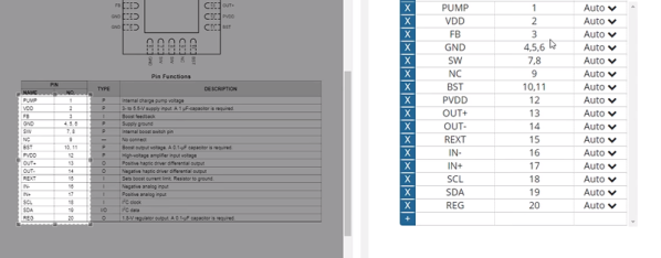
One of the big problems with doing PCB layout is finding a suitable footprint for the components you want to use. Most tools have some library although — of course — some are better than others. You can often get by with using some generic footprint, too. That’s not handy for schematic layout, though, because you’ll have to remember what pin goes where. But if you can’t find what you are looking for SnapEDA is an interesting source of components available for many different layout tools. What really caught our eye though was a relatively new service they have that uses computer vision and OCR to generate schematic symbols directly from a data sheet. You can see it work in the video below.
The service seems to be tied to parts the database already knows about. and has a known footprint available. As you’ll see in the video, it will dig up the datasheet and let you select the pin table inside. The system does OCR on that part of the datasheet, lets you modify the result, and add anything that it missed.
Arguably the biggest hurdle to implanted electronics is in the battery. A modern mobile phone can run for a day or two without a charge, but that only needs to fit into a pocket and were its battery to enter a dangerous state it can be quickly removed from the pocket. Implantable electronics are not so easy to toss on the floor. If the danger of explosion or poison isn’t enough, batteries for implantables and ingestibles are just too big.
Researchers at MIT are working on a new technology which could move the power source outside of the body and use a wireless power transfer system to energize things inside the body. RFID implants are already tried and tested, but they also seem to be the precursor to this technology. The new implants receive multiple signals from an array of antennas, but it is not until a couple of the antennas peak simultaneously that the device can harvest enough power to activate. With a handful of antennas all supplying power, this happens regularly enough to power a device 0.1m below the skin while the antenna array is 1m from the patient. Multiple implants can use those radio waves at the same time.
The limitations of these devices will become apparent, but they could be used for releasing drugs at prescribed times, sensing body chemistry, or giving signals to the body. At this point, just being able to get the devices to turn on so far under flesh is pretty amazing.
Recently, we asked what you thought of the future of implanted technology and the comment section of that article is a treasure trove of opinions. Maybe this changes your mind or solidifies your opinion.
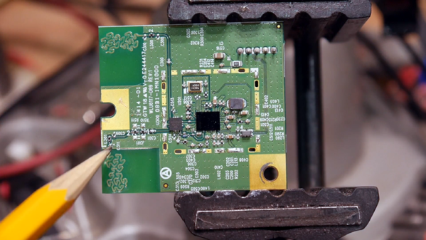
[IMSAI Guy] tore apart a device with a wireless network card and decided to investigate what was under the metal can. You can see the video of his examination below. Overall, it was fairly unremarkable, but one thing that was interesting was its use of an antenna on the PCB that uses a fractal design.
You probably know fractals are “self-similar” in that they are patterns made of smaller identical patterns. The old joke is that the B. in Benoit B. Mandelbrot (the guy who coined the term fractal) stands for Benoit B. Mandelbrot. You can think of it as akin to recursion in software. Antennas made with fractal patterns have some unusual and useful properties.
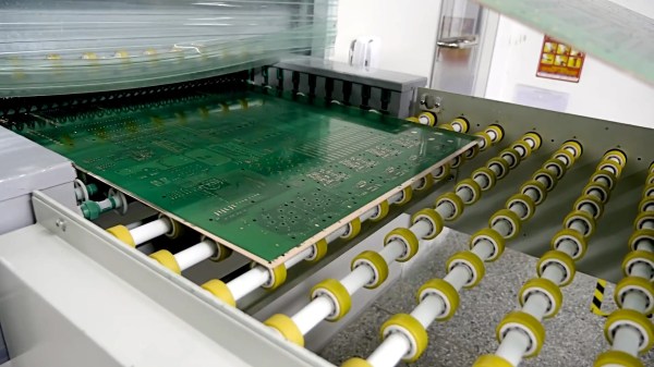
The availability of low-cost, insanely high-quality PCBs has really changed how we do electronics. Here at Hackaday we see people ditching home fabrication with increasing frequency, and going to small-run fab for their prototypes and projects. Today you can get a look at the types of factory processes that make that possible. [Scotty Allen] just published a (sponsored) tour of a PCB fab house that shows off the incredible machine tools and chemical baths that are never pondered by the world’s electronics consumers. If you have an appreciation PCBs, it’s a joy to follow a design through the process so take your coffee break and let this video roll.
Several parts of this will be very familiar. The photo-resist and etching process for 2-layer boards is more or less the same as it would be in your own workshop. Of course the panels are much larger than you’d ever try at home, and they’re not using a food storage container and homemade etchant. In fact the processes are by and large automated which makes sense considering the volume a factory like this is churning through. Even moving stacks of boards around the factory is show with automated trolleys.
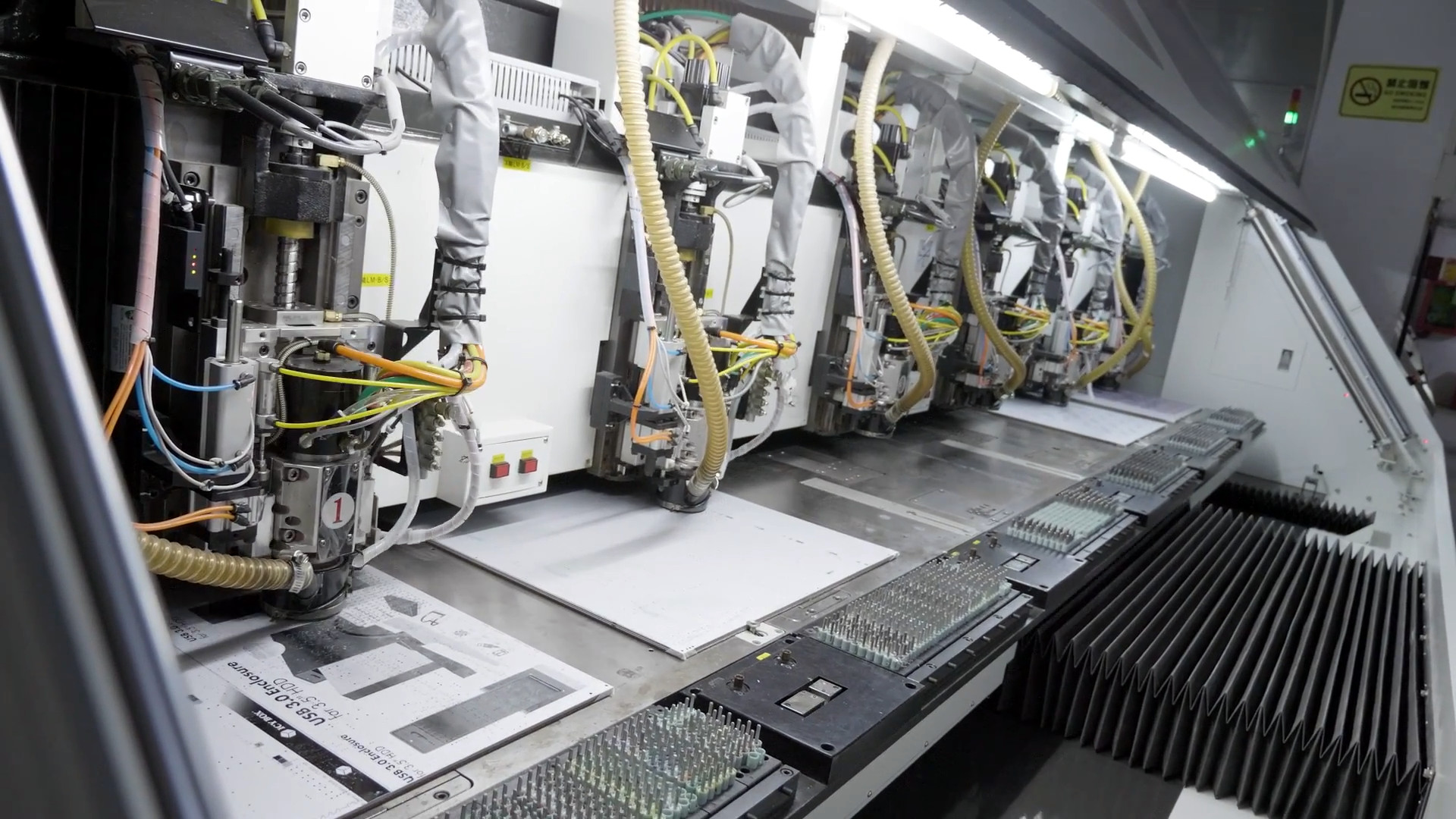
Six headed PCB drilling machine (four heads in use here).
What we find most interesting about this tour is the multi-layer board process, the drilling machines, and the solder mask application. For boards that use more than two layers, the designs are built from the inside out, adding substrate and copper foil layers as they go. It’s neat to watch but we’re still left wondering how the inner layers are aligned with the outer. If you have insight on this please sound off in the comments below.
The drilling process isn’t so much a surprise as it is a marvel to see huge machines with six drill heads working on multiple boards at one time. It sure beats a Dremel drill press. The solder mask process is one that we don’t often see shown off. The ink for the mask is applied to the entire board and baked just to make it tacky. A photo process is then utilized which works much in the same way photoresist works for copper etching. Transparent film with patterns printed on it cures the solder mask that should stay, while the rest is washed away in the next step.
Boards continue through the process to get silk screen, surface treatment, and routing to separate individual boards from panels. Electrical testing is performed and the candy making PCB fab process is complete. From start to finish, seeing the consistency and speed of each step is very satisfying.
Right now, we’re running the greatest hardware competition on the planet. The Hackaday Prize is the Academy Awards of Open Hardware, and we’re opening the gates to thousands of hardware hackers, makers, and artist to create the next big thing.
Last week, we wrapped up the second challenge in The Hackaday Prize, the Robotics Module challenge. Now we’re happy to announce twenty of those projects have been selected to move onto the final round and have been awarded a $1000 cash prize. Congratulations to the winners of the Robotics Module Challenge portion of the Hackaday Prize. Here are the winners, in no particular order:
That the Cold War was a tense and perilous time in history cannot be denied, and is perhaps a bit of an understatement. The world stood on the edge of Armageddon for most of it, occasionally stepping slightly over the line, and thankfully stepping back before any damage was done.
As nerve-wracking as the Cold War was, it had one redeeming quality: it turned us into a spacefaring species. Propelled by national pride and the need to appear to be the biggest kid on the block, the United States and the Soviet Union consistently ratcheted up their programs, trying to be the first to make the next major milestone. The Soviets made most of the firsts, making Sputnik and Gagarin household names all over the world. But in 1962, they laid down a marker for a first of epic proportions, and one that would sadly stand alone for the next 19 years: they put the first woman, Valentina Tereshkova, into space.
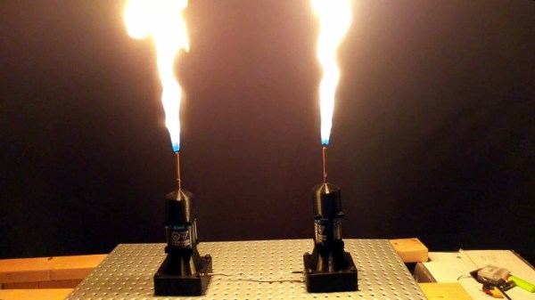
We all have a weakness for a good flamethrower project, but sometimes they can look a little hairy, even if losing hairs to them seems to be the order of the day. [Hyper_Ion] has a ‘thrower that might satisfy the need for fire among the cautious though, because he’s created a remote control flamethrower.
Fuel for the flames is provided from a butane canister held within a 3D-printed frame, and is delivered via a piece of copper tube to a welding nozzle. A plunger beneath the can is connected to a rack-and-pinion driven by a servo, connected to a straightforward radio control receiver. The position of the can is adjusted until there is just enough gas to sustain a pilot flame at the nozzle, and a command to the servo releases a burst of gas that results in a satisfying puff of fire.
This is more of a static stage effect than the wearable flamethrowers or flamethrower guitar projects we’ve seen in the past, but it is no less a neat project. And unlike many other flamethrowers, it’s simple to build. We have to deliver the usual exhortation though: take care with your fire, we’d prefer not to be writing either obituaries of Fail Of The Week posts about smoking ruins.