KiCad 2022 Year End Recap

KiCad 2022 End-of-Year Recap And 7.0 Preview

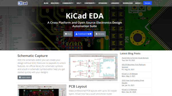
[Chris Gammell] moderated the KiCad 2022 End-of-Year Recap with several KiCad developers and librarians. They reviewed what’s been bubbling up in the nightly KiCad 6 builds, what we can expect from KiCad 7, and even answered some questions from the user community. Over the course of 2022, the KiCad project has grown both its development team and library team. The project even has a preliminary support commitment from the CERN Drawing Office!

Improvements to the KiCad Schematic Editor include smart wire dragging that simplifies moving components around within schematic diagrams. Components selected in the schematic now remain selected while switching to the PCB Editor. Internal documentation of schematics has advanced with support for fonts, embedded graphics, and the inclusion of hypertext links to datasheets and other reference materials. New features for PDF generation offer interactive files and links between sheets.

A new search panel within the KiCad PCB Editor supports finding components by footprint, net, or text search. A property panel allows common properties to be edited across multiple selected items. While a full-blown auto-router remains outside of the scope for KiCad, “push and shove” routing is faster and easier. An “attempt to finish” feature routes a quick connection for the currently selected trace, and “pack and move” positions all selected footprints into proximity to simplify placing them as neighbors within the board layout.

The KiCad PCB Editor also adds support for the use of fonts and inverted “knockout text” which even works on copper zones. Bitmap graphics can be imported and scaled beneath layout work as reference illustrations. Private footprint layers can be used to place extra documentation within footprints. The design rule checker (DRC) now can catch more layout issues, especially those that may impact manufacturability.

These are just a sampling of the impressive improvements we can expect with KiCad 7.0. There are also additions to circuit simulation and modeling features, a new command line interface for script-based automation, ARM64 support for KiCad running on Apple silicon, and a huge number of additions to the default library including symbols, footprints, and 3D Viewer models.

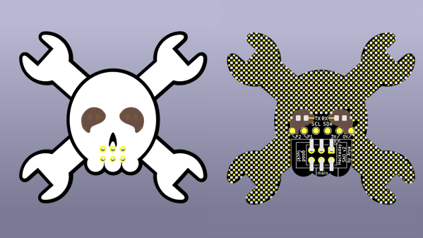
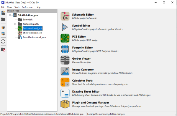
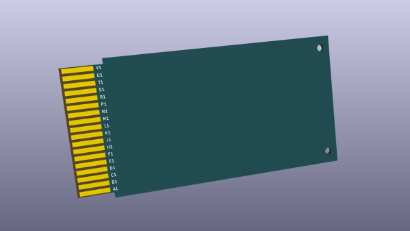
The KiCad team suggests several ways to support the project. There are always needs for additional developers and librarians. Financial contributions can be made at kicad.org. As users, we can run the nightly builds, try to break them, and give feedback in the form of detailed bug reports. Community testing will help make KiCad 7.0 as solid as possible. The project team is also seeking open hardware projects to include with KiCad 7.0 as demos.  For example, the StickHub project was included with KiCad 6.0 as a demo.

The official release of KiCad 7.0 is currently scheduled for January 31, 2023. While we wait, let’s flashback to our January 2022 presentation of what features made it into the KiCad 6.0 release.

Continue reading “KiCad 2022 End-of-Year Recap And 7.0 Preview”

front and back of the Jolly Wrencher SAO

Jolly Wrencher SAO, And How KiCad 6 Made It Easy

If you plan to attend Supercon or some other hacker conference, know that you’re going to get a badge with a SAO (Simple Add-On) connector, a 4-pin or 6-pin connector that you can plug an addon board onto. There’s myriads of SAOs to choose from, and if you ever felt like your choice paralysis wasn’t intense enough, now you have the option of getting a Jolly Wrencher SAO board!

This board gives you an SMD prototyping space, with 1.27mm (0.05″ pitch) pads, suitable for many passive components, ICs and even modules like the ESP32 WROOM. Those pads are diagonally interspersed with ground-fill-connected pads – if you want to bodge something on the spot, you don’t need to pull separate GND wires. Given the Supercon badge specifics, the SAO-standard SDA and SCL pins have RX and TX labels as well. For bonus points, the eyes are transparent, with LED footprints behind them – it’s my first time designing a PCB where the LED shines through the FR4, and I hope that the aesthetics work out!

This design is open with gerber files available for download, so if you thought of making a quick PCB order, I’m giving you one more .zip file to add to it. Otherwise, it’s possible that you will find a Wrencher board lying around at Supercon! Now, I’d like to tell you how KiCad 6 made it super easy to design this PCB – after all, there’s never enough SAOs, and it’s quite likely you’ll want to design your own special SAO, too.

Continue reading “Jolly Wrencher SAO, And How KiCad 6 Made It Easy”

KiCAD Plugin Gives Your PCBs That Handmade Look

The first PCBs we built involved a draftsman laying out large pieces of tape. The finished artwork would be photographically reduced to produce the board. This solved a few problems. It was easier to work on the large pieces and any errors were reduced by the scale amount. Boards from this era have a distinct appearance because the tracks are generally curved. But when computer-aided drafting took over, the early packages couldn’t deal with wavy lines making all sorts of angles. So traces started appearing at very common angles like 45 degrees or 90 degrees only. If you use KiCAD, though, there’s no reason to have rectilinear traces. Now there is a plugin to help make your boards appear like old-fashioned circuit boards.

The video by [mitxela] below talks about how we got here and debunks some common myths about PCB design. The plugin produces rounded corners and teardrop-shaped pads. There’s also a second post on the topic with more details. The effect isn’t just ornamental. There are some reasons graceful traces might be better than sharp angles.

Continue reading “KiCAD Plugin Gives Your PCBs That Handmade Look”

KiCAD 6.0: What Made It And What Didn’t

I’ve been following the development of KiCAD for a number of years now, and using it as my main electronics CAD package daily for a the last six years or thereabouts, so the release of KiCAD 6.0 is quite exciting to an electronics nerd like me. The release date had been pushed out a bit, as this is such a huge update, and has taken a little longer than anticipated. But, it was finally tagged and pushed out to distribution on Christmas day, with some much deserved fanfare in the usual places.

So now is a good time to look at which features are new in KiCAD 6.0 — actually 6.0.1 is the current release at time of writing due to some bugfixes — and which features originally planned for 6.0 are now being postponed to the 7.0 roadmap and beyond. Continue reading “KiCAD 6.0: What Made It And What Didn’t”

Advanced PCB Graphics With KiCAD 6 And Inkscape

There are many, many video tutorials about designing the functional side of PCBs, giving you tips on schematic construction, and layout tips. What is a little harder to find are tutorials on the graphical aspects, covering the process from creating artworks and how you can drive the tools to get them looking good on a PCB, leveraging the silkscreen, solder and copper layers to maximum effect. [Stuart Patterson] presents his guide for Advanced PCB Graphics in KiCAD 6.0 and Inkscape, (Video, embedded below) to help you on your way to that cool looking PCB build.

Silkscreen layers in yellow, solder mask opening in red

The first step is to get your bitmap, whether you create it yourself, or download it, and trace it into a set of vectors using the Inkscape ‘trace bitmap’ tool. If you started with an SVG or similar vector shape, then you can skip that stage.

Next simply create a PCB outline shape by deleting all the details that aren’t part of the outline. A little scaling here and there to get the dimensions correct and you’re done with the first part. [Stuart] has an earlier video showing that process.

The usability improvements in KiCAD 6.0 are many, but one greatly demanded feature is the ability to group objects, just like you do in Inkscape and any other vector graphics tool for that matter. That means you can simply import that SVG outline into the Edge.Cuts PCB layer and all the curves will be nicely tied together. Next you select the details you want for the silkscreen layer, solder mask removal layers and any non-circuit copper. In Inkscape it would be wise to use the layers feature to assign the different material types to a uniquely named layer, so they can be hidden for exporting. This allows you to handle silk, mask and copper PNG exports from a single master file, in addition to any vector details for outline, slots and holes.

Once you have PNG bitmap exports for the silk, mask etc. you need to create a footprint inside a board-specific library, using the KiCAD image converter tool. It was interesting to note that you can export a new image footprint from the tool and paste it straight into the footprint editor, and tweak all the visibility details at the same time. That will save some time and effort for sure. Anyway, we hope this little tutorial from [Stuart] helps, and we will be sure to bring you plenty more in the coming months.

Need some more help with KiCAD? Checkout this tutorial, and if you want a bit more power from the tool, you need some action plugins!

Continue reading “Advanced PCB Graphics With KiCAD 6 And Inkscape”

Flip-Chip KiCad Templates

We like retro-computing and we like open source standards that allow easy project sharing. Vintage DEC computer enthusiast [Jay Logue] combines both of these in his recent project on GitHub, where he shares several KiCad templates for making your own Flip-Chip modules. Although named after the semiconductor packaging technique we are familiar with today, DEC Flip-Chips were introduced in 1964 as a modular electronics packaging system. These were used in many of DEC’s Programmable Data Processor (PDP) computers, beginning with the PDP-8 in 1965. DEC also had a Digital Laboratory Module family, which was a roll-your-own custom electronic system. The 1968 Digital Logic Handbook shows the available modules, and has the look and feel of the TTL Cookbook book which would come along six years later.

Flip-Chips came in a variety of sizes over the years: single-, double-, and quad-, and hex-height boards having standard- and extended-length. The PCB’s have 18 gold-plated fingers on one edge, later extended to 36 fingers double-sided, which plug into a backplane. Interconnections were typically wire-wrapped. A single height board is 127 x 62 mm (5 x 2-7/16 inches) with a labeled extractor bracket on one end. [Jay]’s repository has templates for five of the most popular variations, and making other sizes should be straightforward using these templates as a starting point.

Continue reading “Flip-Chip KiCad Templates”

an image of kicad's homepage

KiCad Team Releases Warning Regarding Domain Name

On October 19th, [Seth_h] from the KiCad Project posted on the KiCad forums that the project’s original domain name kicad-pcb.org has been unexpectedly sold to a third party, and urged members of the community to avoid any links to this old website.

KiCad has used the domain kicad-pcb.org since 2012 as the official source for information on and downloads of their popular open-source electronics design software. Unfortunately, the original domain name was purchased before KiCad was formalized as an organization, so it was not directly under their control. This all came to head when the old domain name was unexpectedly sold to an unnamed third party that was not affiliated with the project. Currently, the old domain is just a website covered in ads, but the KiCad team fears that it may be used maliciously in the future.

With KiCad’s popularity, thousands of tutorials, articles, and project guides over the years have included links to the old KiCad domain. A Google search in October 2021 found more than 19,000 instances of the old domain spread across the internet. [Seth_h] has called upon the community to make every effort possible to update old links, reducing the chance that people stumble across the wrong website.

[Editor’s Note: We think we got ’em all, let us know if we missed any.]

Luckily, Digikey has swooped in to help save the day. They purchased a new domain, kicad.org, from squatters and donated it to the KiCad Project. (Update: Digi-key donated the KiCad.org domain back in October of 2020 after noticing fishy squatters going back to at least 2016) [Seth_h] explains in his post that a number of safeguards have been put in place to prevent this from happening in the future, including not having the domain name owned by a single person, and having all KiCad trademarks registered to the Linux Foundation.

There’s a good reason why KiCad has gotten so popular, it is packed full of great features for PCB design. Check out our coverage of some of the new features we are most excited for in KiCad 6.0 here.