We’re not exactly what you’d call naturalists here at Hackaday, so to us, the idea that hot pepper seeds need to germinate in hot conditions sounds suspiciously like a joke. The sort of thing somebody might tell you right before they try to sell you an elevator pass, or cram you into a locker. But we don’t think [Dean] would have gone through so much trouble if it wasn’t true. You’re still not going to sell us an elevator pass, though. Not again.
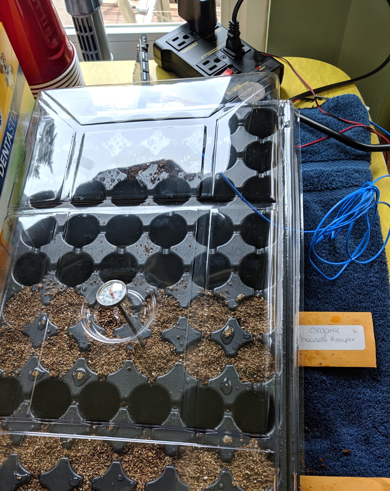
According to [Dean], the Carolina Reaper pepper seeds he bought from Puckerbutt Pepper Company (truly a name you can trust) recommend that they be germinated at a temperature between 80 and 85 degrees Fahrenheit for up to eight weeks. To make sure they were maintained at the optimal temperature for as long as possible, he decided to get a heating pad he could place under the seeds to keep them warm. He just needed some way to make sure the heat only kicked on once the soil temperature fell out of the sweet spot.
To get an accurate reading, [Dean] ended up going with a waterproof K-type thermocouple connected to a SainSmart MAX6675 module that could be buried amongst the seeds. When the soil temperature drops below 82.5 F, it kicks on the heating mat through an IoT Relay by Digital Loggers. He even added in a capacitive soil moisture sensor and a couple of LEDs so he could tell from across the room if he needed to water what he loving refers to as his “Hell Berries”
Cyphercon 4.0 came to life in Milwaukee, Wisconsin on Thursday and the conference badge is a brilliant and engaging design. At first glance it looks like a fairly mundane rectangular badge. But a closer look reveals simplistic elegance wrapping around some clever mechanical design and the awesome interactive mechanism of being able to read paper tape.
That’s right, this badge can read the series of holes punched in the long paper strips you normally associate with old iron of 50 years ago.
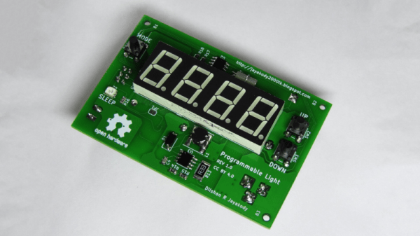
Everything’s internet connected these days, garage doors, baby monitors, and the kitchen sink are all hooked up. There are benefits to having everything online, but also several pitfalls. Maintaining security on a home network is an ongoing job, made more difficult by the number of devices that must be kept track of. Sometimes all the hassle isn’t worth it, and you just want a non-connected solution. [Dilshan] found himself in just that camp, and built a simple programmable light controller that doesn’t connect to the Internet.
At the core of the project is an ATMEGA8 microcontroller, which is cheap, readily available, and can do the job. It’s combined with a DS1307 real time clock IC to keep track of time. The circuit is designed for 24V power, to allow it to be run from the same supply as the LED light modules it is designed to control.
The design was initially prototyped with through-hole parts on the breadboard, with the final design being built with surface mount parts on a custom PCB. Light is courtesy of a 7W warm white LED module. 3 push buttons and a 4-digit, 7-segment display act as the user interface, with an LDR to allow the light to also react to its surroundings.
It’s a build that goes against current trends, lacking WiFi connectivity, Twitter functionality, or cloud-based logging. It goes to show that the right solution isn’t always putting everything online. Sometimes the old methods are enough to do the job, and do it well.
Over the past 30 years the price of hardware has slowly but surely come down, and it’s now possible to buy all manner of widgets and gizmos online for less than the price of a fancy Italian dinner. By and large this is a good thing, but it’s not uncommon to find that your new tools are let down by the software side of things. Of course, you can always develop your own solution – and in [ThePhil]’s case, that’s exactly what he did.
The hardware in question was a PCE-174 luxmeter, which came with an uncooperative Windows application as standard. This simply wouldn’t do, so [ThePhil] set about developing a Linux version in Python. This was achieved through the aid of documentation, not of the PCE-174, but its sibling from another corporation – the Extech HD450. The two meters were similar enough that the Extech’s better documentation was able to fill in the gaps of [ThePhil]’s understanding.
[ThePhil] has diligently implemented the full feature set of the PCE-174, and has documented the project well. There are even notes on the version numbers of various dependencies, which will surely be a great help if someone’s trying to run the code five years down the track.
It’s a great lesson that one need not be at the mercy of the software one is given. For a great many cases, it’s possible to roll your own solutions that are robust and get the job done. This approach can be taken to great lengths – you can go so far as replacing an entire camera firmware, if you so wish.
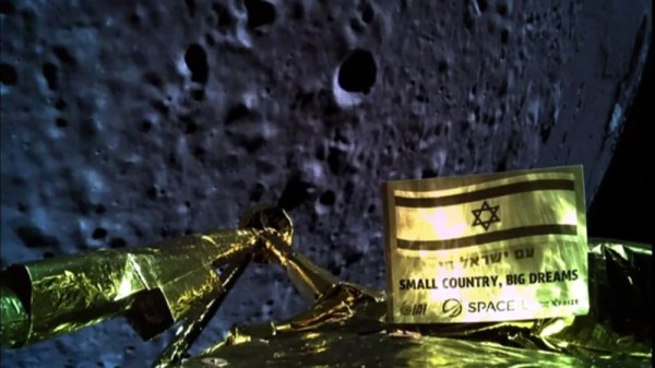
Some bittersweet news today as we get word that Israel’s Beresheet spacecraft unfortunately crashed shortly before touchdown on the Moon. According to telemetry received from the spacecraft right up until the final moments, the main engine failed to start during a critical braking burn which would have slowed the craft to the intended landing velocity. Despite attempts to restart the engine before impact with the surface, the craft hit the Moon too hard and is presumably destroyed. It’s likely that high resolution images from the Lunar Reconnaissance Orbiter will eventually be able to give us a better idea of the craft’s condition on the surface, but at this point the mission is now officially concluded.
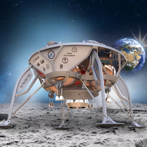
The Beresheet Lander
It’s easy to see this as a failure. Originally conceived as an entry into the Google Lunar X Prize, the intended goal for the $100 million mission was to become the first privately funded spacecraft to not only touch down on the lunar surface, but navigate laterally through a series of powered “hops”. While the mission certainly fell short of those lofty goals, it’s important to remember that Beresheet did land on the Moon.
It didn’t make the intended soft landing, a feat accomplished thus far only by the United States, Russia, and China; but the fact of the matter is that a spacecraft from Israel is now resting on the lunar surface. Even though Beresheet didn’t survive the attempt, history must recognize Israel as the fourth country to put a lander on the surface of our nearest celestial neighbor.
It’s also very likely this won’t be the last time Israel reaches for the Moon. During the live broadcast of the mission, after it was clear Beresheet had been lost, Prime Minister Benjamin Netanyahu vowed his country would try again within the next two years. The lessons learned today will undoubtedly help refine their next mission, and with no competition from other nations in the foreseeable future, there’s still an excellent chance Israel will be able to secure their place in history as the fourth country to make a successful soft landing.
Beresheet’s view during descent
Of course you’ve got to get to the Moon before you can land on it, and in this respect, Beresheet was an unmitigated success. We previously covered the complex maneuvers required to put the craft into lunar orbit after riding to space as a secondary payload on the Falcon 9 rocket; a technique which we’ll likely see more of thanks to the NASA’s recent commitment to return to the Moon. Even if Beresheet never attempted to land on the surface, the fact that it was able to enter into a stable lunar orbit and deliver dramatic up-close images of the Moon’s surface will be a well deserved point of pride for Israel.
This won’t be the last time that hundreds of millions of dollars worth of high-tech equipment will be lost while pushing the absolute edge of the envelope, and that’s nothing to be upset over. Humans have an insatiable need to see what’s over the horizon and that means we must take on a certain level of risk. The alternative is stagnation, and in the long run that will cost us a lot more than a few crashed probes.
The ESP family of microcontrollers is absolutely on fire right now, with a decent chunk of the projects that come our way now based on one of the impossibly cheap WiFi-enabled boards. In fact, they are so cheap and popular that we’ve started to see a somewhat unexpected trend; people have a tendency to use them as drop-in replacements, despite the more modern boards being considerably more powerful than required. The end result is a bunch of projects in which the ESP is simply underutilized. It’s not a big deal, but somewhat disappointing to see.
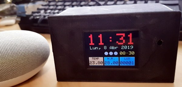
But we can assure you this ESP32 alarm clock created by [Pangodream] is absolutely not one of them. He’s packed an impressive number of features into this unassuming little timepiece, and it’s really an excellent example of how much these boards are capable of without breaking a sweat. From DIY touch sensors to the Android application used to configure the clock over the network, this project is overflowing with neat hardware and software tricks worth taking a closer look at.
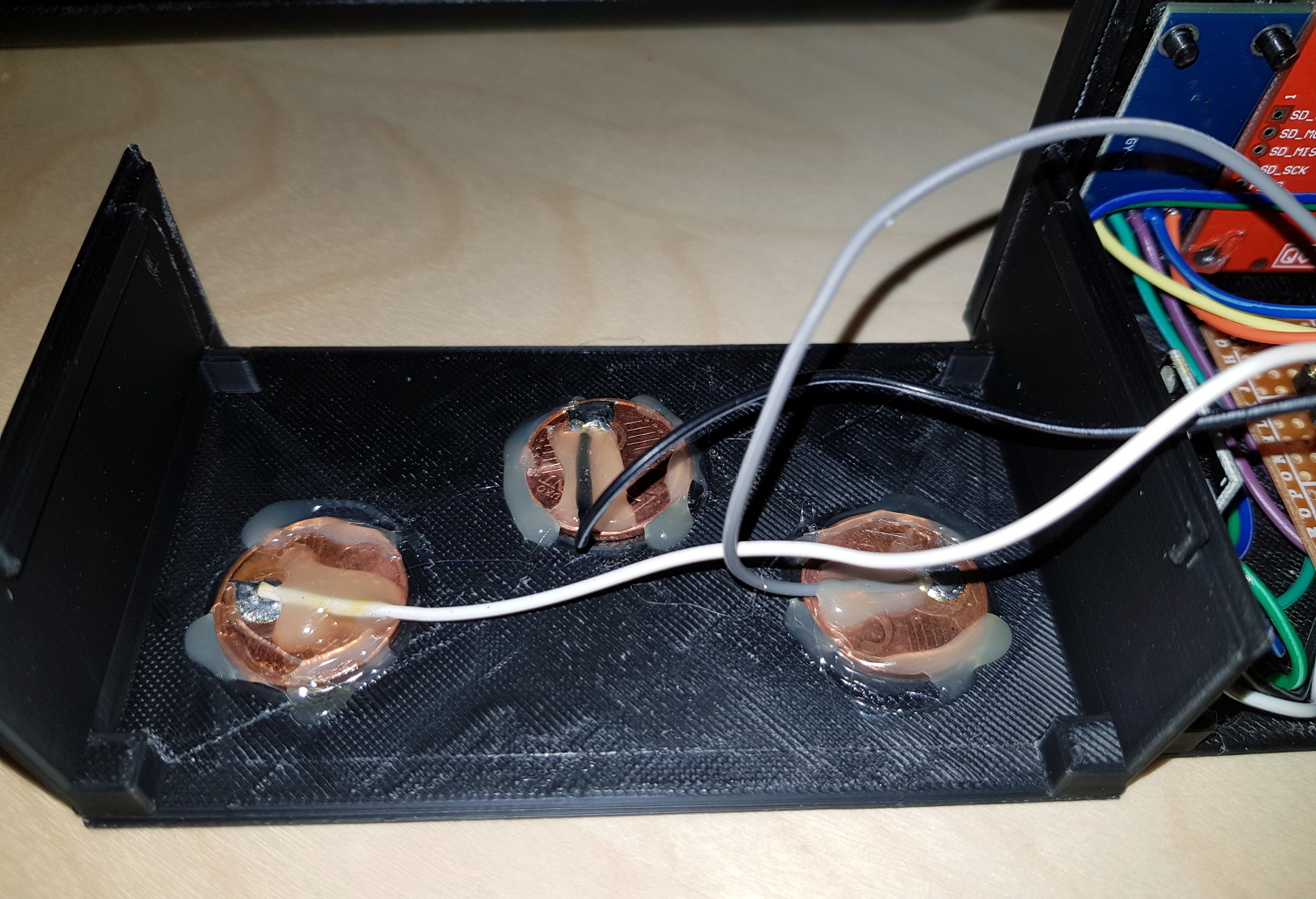
Inside the 3D printed case, the clock features a BH150 light sensor, the very popular DHT-11 for detecting temperature and humidity, as well as a ILI9341 2.8 inch LCD for the display. In a particularly clever touch (get it?), [Pangodream] used three coins connected to the digital pins of the ESP32 as capacitive sensors. These allow him to interact with the click just by tapping the top of the case, and saved him the trouble of adding traditional switches or buttons. We might have put some indentations in the top case to make identifying which of the three “buttons” you’re pushing, but we suppose the invisible interface does make things look a little more futuristic.
But if even that is too much physical touching for you, then [Pangodream] has come up with a fairly robust system for controlling and interacting with the clock over the network. It’s not just a convenient way of setting the time, a good number of the clock’s functions can be polled and configured in this manner; everything from the sensitivity of the touch sensors to how many times it will beep when the alarm goes off. To make things easier, he’s even wrapped it all up in a handy Android application for on the go configuration.
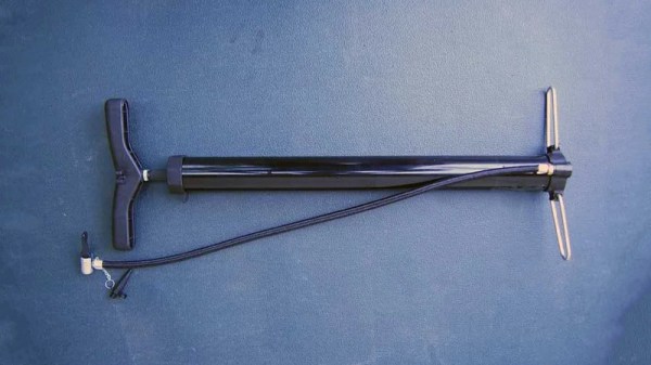
Pulling a vacuum is something every proud maker must do once in a while. Whether you’re degassing epoxy or vacuum forming parts, you’ll need a reliable pump to get the job done. [drcrash] has just the guide to help – on how to convert a regular handpump to vacuum duty. (Video embedded after the break.)
[drcrash] recommends starting with a Slime brand 2060-A pump or similar. It’s a basic hand pump, with no pressure gauges or other frills to get in the way. It’s also got a strong steel shaft that can hold up to repeated use. You’ll also need some tubing and a check valve to get the job done.
The basic concept is to reconfigure the pump to suck air out of things rather than blowing it into them. By removing the original check valve and installing one in the opposite direction, and reversing the pump’s piston, it’s possible to pull good vacuum without breaking a sweat. [drcrash] reports that it’s possible to go up to 11 psi below atmospheric with this setup, which is plenty for a wide range of applications. If you need to go further, you can try building your own turbomolecular pump instead.
 According to [Dean], the Carolina Reaper pepper seeds he bought from Puckerbutt Pepper Company (truly a name you can trust) recommend that they be germinated at a temperature between 80 and 85 degrees Fahrenheit for up to eight weeks. To make sure they were maintained at the optimal temperature for as long as possible, he decided to get a heating pad he could place under the seeds to keep them warm. He just needed some way to make sure the heat only kicked on once the soil temperature fell out of the sweet spot.