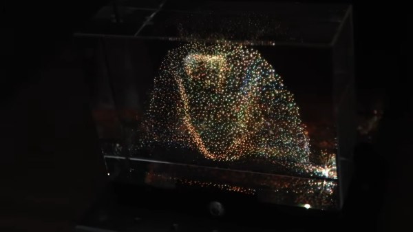
Laser Engraver Uses All Of The DVD Drive

For the last ten to fifteen years, optical drives have been fading out of existence. There’s little reason to have them around anymore unless you are serious about archiving data or unconvinced that streaming platforms will always be around. While there are some niche uses for them still, we’re seeing more and more get repurposed for parts and other projects like this tabletop laser engraver.

The build starts with a couple optical drives, both of which are dismantled. One of the shells is saved to use as a base for the engraver, and two support structures are made out of particle board and acrylic to hold the laser and the Y axis mechanism. Both axes are made from the carriages of the disassembled hard drives, with the X axis set into the base to move the work piece. A high-output laser module is fitted to the Y axis with a heat sink, and an Arduino and a pair of A4988 motor controllers are added to the mix to turn incoming G-code into two-dimensional movement.

We’ve actually seen a commercial laser engraver built around the same concept, but the DIY approach is certainly appealing if you’ve got some optical drives collecting dust. Otherwise you could use them to build a scanning laser microscope.

Continue reading “Laser Engraver Uses All Of The DVD Drive”

Stack of Si3N4-LiNbO3 forming the integrated laser and integrated into test setup (d). (Credit: Snigirev et al., 2023)

Fast Adjustable Lasers Using Lithium Niobate Integrated Photonics

Making lasers smaller and more capable of rapidly alternating between frequencies, while remaining within a narrow band, is an essential part of bringing down the cost of technologies such as LiDAR and optical communication. Much of the challenge here lies understandably in finding the right materials that enable a laser which incorporates all of these properties.

A heterogeneous Si3N4–LiNbO3 chip as used in the study. (Credit: Snigirev et al., 2023)

Here a recent study by [Viacheslav Snigirev] and colleagues (press release) demonstrates how combining the properties of lithium niobate (LiNbO3) with those of silicon nitride (Si3N4) into a hybrid (Si3N4)–LiNbO3 wafer stack allows for an InP-based laser source to be modulated in the etched photonic circuitry to achieve the desired output properties.

Much of the modulation stability is achieved through laser self-injection locking via the microresonator structures on the hybrid chip. These provide optical back reflection that forces the laser diode to resonate at a specific frequency, providing the frequency lock. What enables the fast frequency tuning is that this is determined by the applied voltage on the microresonator structure via the formed electrodes.

With a LiDAR demonstration in the paper that uses one of these hybrid circuits it is demonstrated that the direct wafer bonding approach works well, and a number of optimization suggestions are provided. As with all of these studies, they build upon years of previous research as problems are found and solutions suggested and tested. It would seem that thin-film LiNbO3 structures are now finding some very useful applications in photonics.

(Heading image: Stack of Si3N4-LiNbO3 forming the integrated laser and integrated into test setup (d). (Credit: Snigirev et al., 2023) )

DIY Laser For Ablating Metal

For those who wish to go beyond through-hole construction on perfboard for their circuit boards, a printed circuit board is usually the next step up. Allowing for things like surface-mount components, multi-layer boards, and a wider array of parts, they are much more versatile but do have a slight downside in that they are a little bit harder to make. There are lots of methods for producing them at home or makerspace, though, and although we’ve seen plenty of methods for their production like toner transfer, photoresist, and CNC milling, it’s also possible to make them using laser ablation, although you do need a special laser to get this job done.

The problem with cutting copper is that it reflects infra-red, so a higher-wavelength blue green laser is used instead. And because you want to ablate the copper, but not melt the surrounding areas or cut straight through the board, extremely short, high-power pulses are the way to go. Here, the [Munich Fab Lab] is using 9 kW pulses of around 30 microseconds each.  With these specifications the copper is ablated from the surface of the board allowing for fine details in the range of about 20 µm, which is fine enough for just about any circuit board. The design of the laser head itself is worth a look.

Aside from the laser, the rest is standard CNC machine fodder, but with an emphasis on safety that’s appropriate for a tool in a shared workspace, and the whole project is published under an open license and offers an affordable solution for larger-scale PCB production with extremely fine resolution and without the need for any amounts of chemicals for the more common PCB production methods. There is a lot more information available on the project’s webpage and its GitHub page as well.

Of course, there are other methods of producing PCBs by laser if you happen to have a 20 W fiber laser just kicking around.

No Moving Parts LiDAR

Self-driving cars often use LiDAR — think of it as radar using light beams. One limitation of existing systems is they need some method of scanning the light source around, and that means moving parts. Researchers at the University of Washington have created a laser on a chip that uses acoustic waves to bend the laser, avoiding physically moving parts. The paper is behind a paywall, but the University has a summary poster, and you can also find an overview over on [Geekwire].

The resulting IC uses surface acoustic waves and can image objects more than 100 feet away. We would imagine this could be helpful for other applications like 3D scanning, too. The system weighs less than a conventional setup, too, so that would be valuable in drones and similar applications.

Continue reading “No Moving Parts LiDAR”

Growing Simple Crystals For Non-Linear Optics Experiments

Here’s an exercise for you: type “crystals” into your favorite search engine and see what you get. If you’re anything like us, you’ll get a bunch of pseudoscientific posts about the healing power of crystals, along with offers to buy the same at exorbitant prices. But woo-woo aside, certain crystals do have seemingly magical powers — like the ability to turn light from one color into another.

None of this is magic, of course. Rather, as optics aficionado [Les Wright] explains, non-linear optics is all about physics. Big physics, too, like the kind that made the National Ignition Facility the first fusion research outfit to reach the “break-even” point, at least in terms of optical energy. To do so, they need to convert megajoules of infrared laser beams all the way across the visible spectrum into the ultraviolet, relying on huge crystals of deuterated potassium dihydrogen phosphate (KDP) to do so. Depending on how they’re cut, crystals of these sorts have non-linear optical properties like second-harmonic generation, which combines two input photons into a single output photon with twice the energy of the original. This results in a halving of the wavelength of the input, which doubles the frequency.

While the process used at the NIF produces crystals of enormous proportions, [Les] has more modest needs and thus a simpler process. His KDP is an off-the-shelf chemical, nothing fancy about it, which is added to boiling water to make a saturated solution. A little of the solution is poured out into a watch glass to make seed crystals, and everything is allowed to cool slowly. A nice seed crystal is glued to a piece of monofilament fishing line and suspended in the saturated solution, and with enough time a good-sized crystal forms. Placed into the beam path of a 1,064 nm IR laser and rotated carefully relative to the beam, the crystal easily produces a brilliant green laser output.

This is fascinating stuff, and we’re looking forward to seeing where [Les] goes with this. Polishing the crystals to make them optically cleaner would be a good next step, as would perhaps growing even larger crystals.

Continue reading “Growing Simple Crystals For Non-Linear Optics Experiments”

TeraByte InfraRed Delivery (TBIRD)

NASA Team Sets New Space-to-Ground Laser Communication Record

[NASA] and a team of partners has demonstrated a space-to-ground laser communication system operating at a record breaking 200 gigabit per second (Gbps) data rate. The TeraByte InfraRed Delivery (TBIRD) satellite payload was designed and built by [MIT Lincoln Laboratory]. The record of the highest data rate ever achieved by a space-to-Earth optical communication link surpasses the 100 Gbps record set by the same team in June 2022.

TBIRD makes passes over an ground station having a duration of about six-minutes. During that period, multiple terabytes of data can be downlinked. Each terabyte contains the equivalent of about 500 hours of high-definition video. The TBIRD communication system transmits information using modulated laser light waves. Traditionally, radio waves have been the medium of choice for space communications. Radio waves transmit data through space using similar circuits and systems to those employed by terrestrial radio systems such as WiFi, broadcast radio, and cellular telephony. Optical communication systems can generally achieve higher data rates, lower loses, and operate with higher efficiency than radio frequency systems. Continue reading “NASA Team Sets New Space-to-Ground Laser Communication Record”

Easy Graphene Production With A Laser Engraver

Graphene isn’t easy to produce at scale. But making small batches of graphene is doable in a few ways. [Robert Murray-Smith] decided to try producing “flash graphene.” This requires a big capacitor bank that is moderately expensive, so he decided to explain a different technique he read about using an ordinary laser cutter. Check it out in the video below.

We were a little disappointed that he didn’t actually make any graphene this time. He has, however, used other methods in other videos to create some type of graphene. In fact, he has many similar videos going back quite a ways as well as applications with concrete, capacitors, and more. We understand that this method doesn’t produce monolayer graphene, but actually creates a graphene “foam” with interesting properties. [Robert] talks about recent papers that show you can grow graphene on things other than Kapton tape using this method.

Continue reading “Easy Graphene Production With A Laser Engraver”