Vintage electronics and capacitor replacements tend to go hand-in-hand. Why? Because electrolytic capacitors just don’t last, not the way most other components do, anyway.
It’s one thing to swap old caps with modern replacements, but what about electronics where the components are not hidden away, and are an important part of the equipment’s look? [lens42] shares a method for replacing antique can-style capacitors in a way that leaves them looking completely original. All it takes is some careful application of technique.
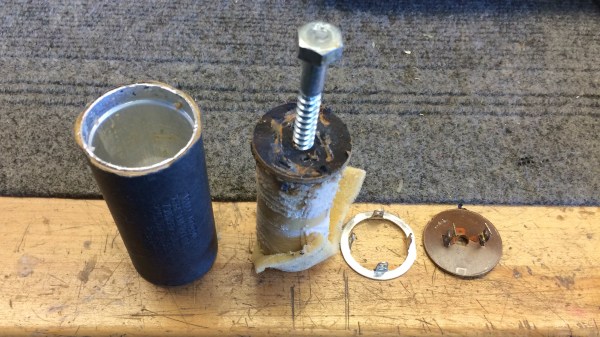
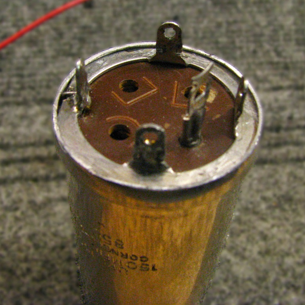
The first thing to do is carefully file away the crimp of the metal can until one can release the ring and plate that hold the terminals. Once that is off, the internals can be pulled from the metal can for disposal. Since the insides of the old cap won’t be re-used, [lens42] recommends simply drilling a hole, screwing in a lag bolt to use as a handle, and pulling everything out. There’s now plenty of space inside the old can to hold modern replacements for the capacitor, and one can even re-use the original terminals.
That leaves the job of re-crimping the old can around the terminal ring to restore a factory-made appearance. To best do this, [lens42] created a tapered collar. Gently hammering the can forces the bottom into the taper, and the opening gradually crimps around the terminal ring. It’s also possible to carefully hammer the flange directly, but the finish won’t be as nice. This new crimp job may not look exactly the same as before, but once the cap is re-installed into the original equipment, it won’t be possible to tell it has been modified in any way.
If this sounds a bit intimidating, don’t worry. [lens42] provides plenty of pictures. And if this kind of thing is up your alley, you may want to check out the Caps Wiki, an effort to centralize and share details about tech repair, especially for vintage electronics.