We’re big fans of repairable hardware here at Hackaday, so much so that when we see a company embracing the idea that their products should actually be serviced rather than thrown in the trash, we like to call attention to it. Yes, that even includes when it’s Microsoft.
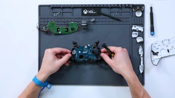
This community has had a mixed relationship with the Redmond software giant, to say the least. But we’ve still got to give them credit when they do something positive. Not only are they offering a full selection of replacement parts for both the standard and Elite Xbox controllers, they’ve also provided written instructions and step-by-step video guides on how to install your new parts.
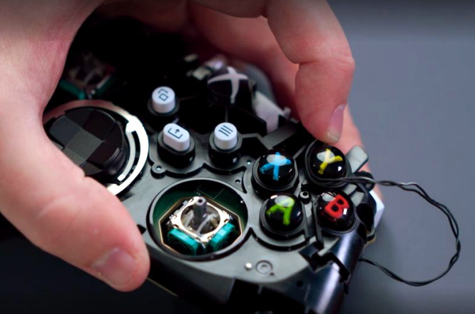 For those of you who stopped playing console games when the controllers still only had two buttons, this might not seem like such a big deal. But considering a new Xbox Elite Wireless Controller will set you back a dizzying $180, it’s not hard to see why some folks would be excited about the possibility of swapping out the guts of the thing for $50.
Of course, these parts were already available from third party sellers, and iFixit naturally has repair guides for all the different flavors of Xbox controllers. Nothing about what Microsoft is doing here makes the Xbox controller fundamentally any easier to repair than it was previously. But the fact that the company isn’t treating their customers like adversaries is a step in the right direction.
Valve has been similarly open about the internals of the Steam Deck, though their presentation was a bit dramatic, and even Sony provided an official teardown video for the PS5. We’re not sure why these companies are willing to pull back the curtain when it comes to gaming hardware. Whatever the reason, we’re certainly not complaining.
Continue reading “Microsoft Now Offering Parts And Repair Guides For Xbox Controllers”