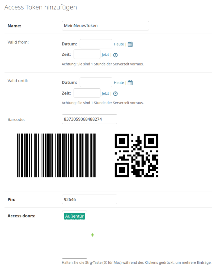
Before it became viable to distribute and play music tracks on home computers, the use of FM and Wavetable synthesis was very common, with MIDI Wavetable-based devices like the Roland MT-32 and SC-55 still highly sought after today. The Creative Midi Blaster MB-10 that [Yeo Kheng Meng] reviewed and tore down for an analysis isn’t quite as famous or sought after, but it provides a good example of what Creative Labs was doing at the time in this space.
Released in 1993, it definitely has more of a popular style vibe to it than the utilitarian Roland devices, even if this means highly impractical curves. In the list of features it claims Roland MT-32 emulation, which would have made it quite a bit more useful to the average user, including gamers of the era. Games like DOOM supported these MIDI devices for audio, for example.
In terms of price only the Roland SC-55ST comes close to the MB-10, similarly dropping a screen and a host of features. In terms of features the MB-10 claims far fewer instruments than the SC-55 variants, with even with the slightly higher priced SC-55ST massively outgunning it in raw specs. So would you ever buy the MB-10 back then and consider it a ‘good deal’? If $100 in 1990s money was worth losing full MIDI compatibility for, then it seems the answer was ‘yes’.
Continue reading “A Look Inside The Creative MB-10 MIDI Blaster”